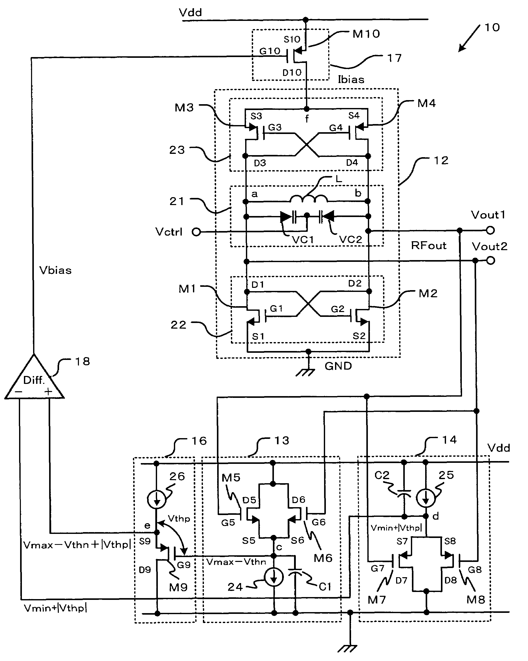
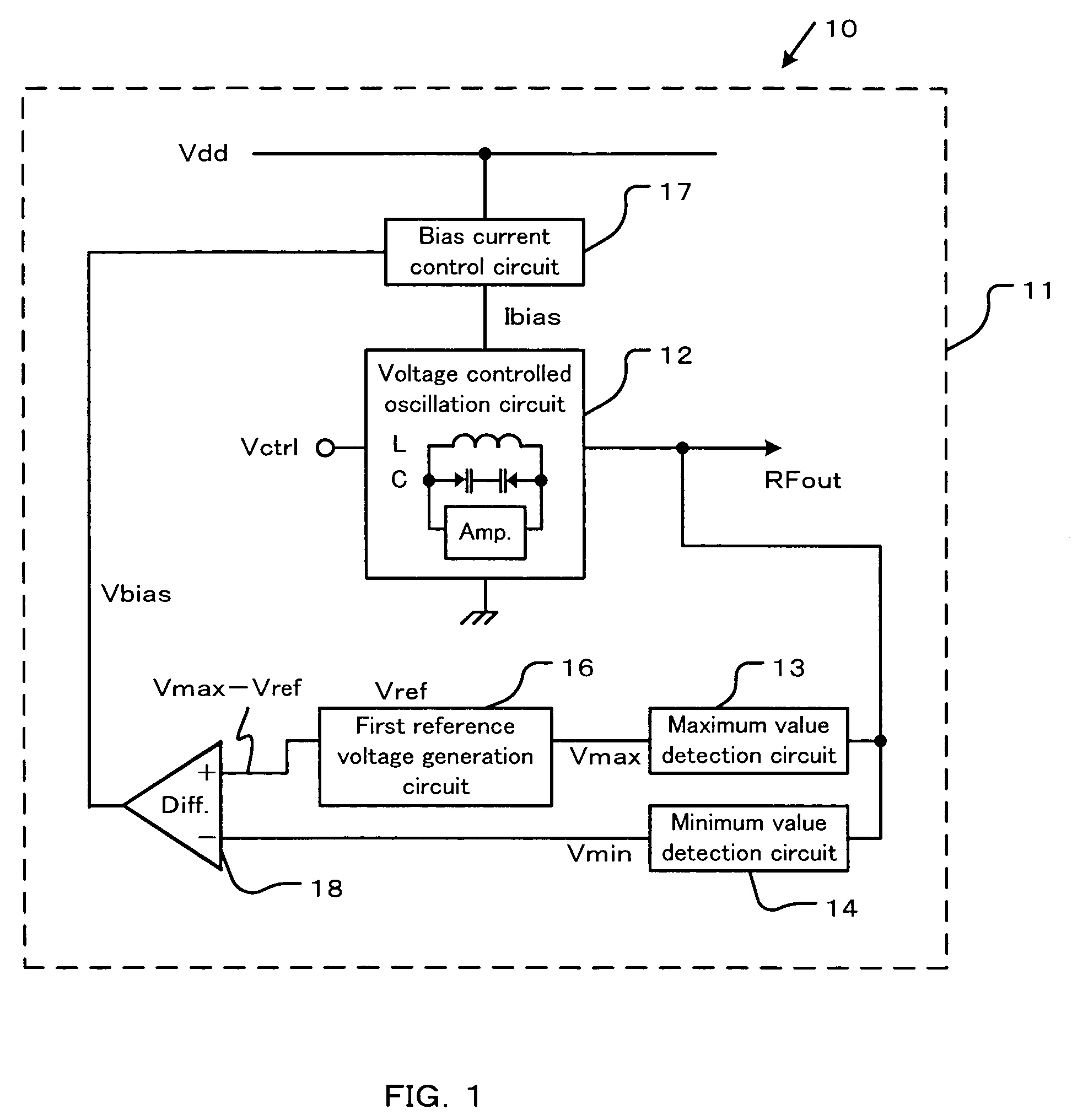
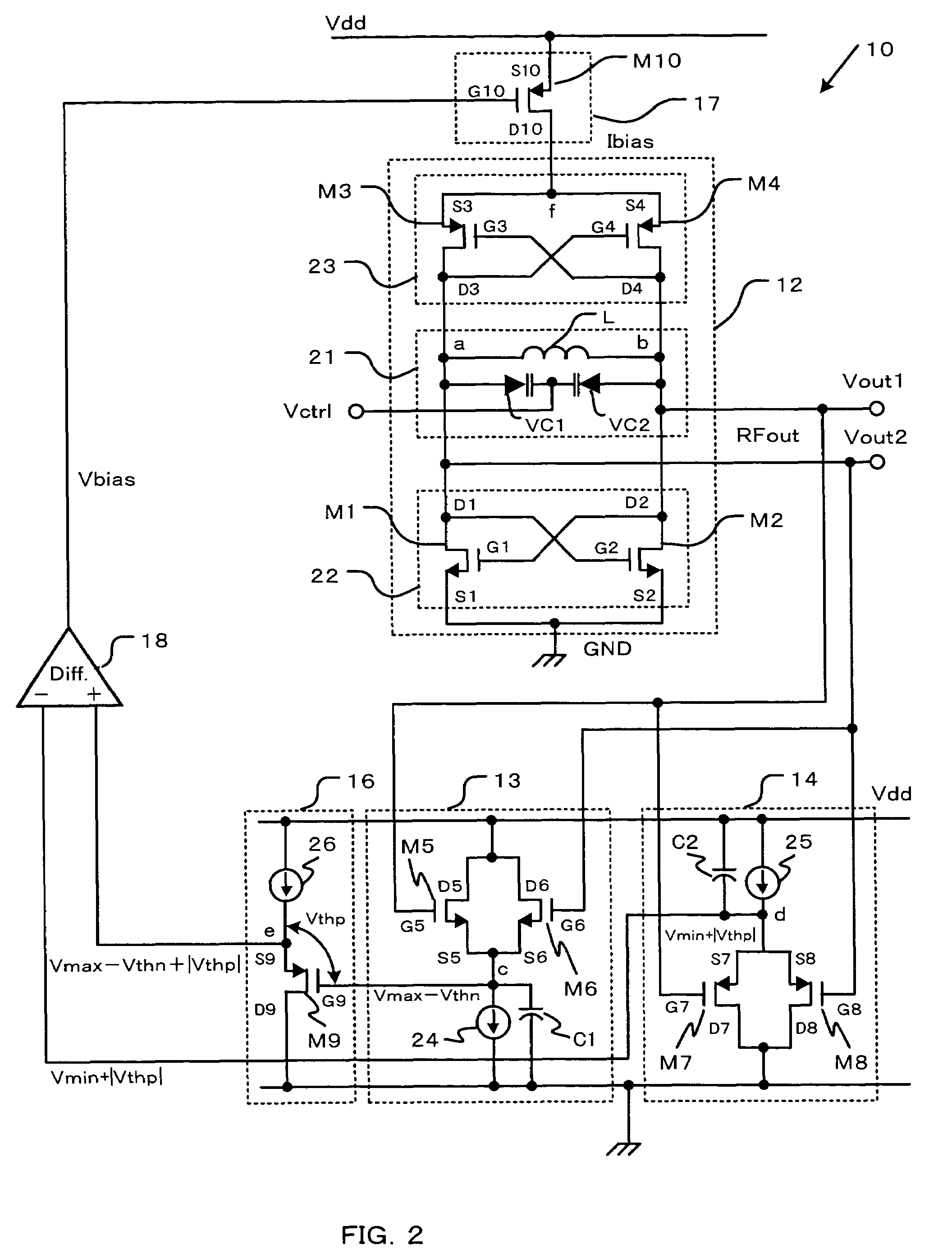
Semiconductor integrated circuit device and wireless communication device
a technology of integrated circuit and wireless communication, which is applied in the direction of oscillator, pulse automatic control, pulse technique, etc., can solve the problems of phase noise performance fluctuation, and phase noise performance deterioration
- Summary
- Abstract
- Description
- Claims
- Application Information
AI Technical Summary
Problems solved by technology
Method used
Image
Examples
first embodiment
[0071]The solid line a shows a result of a simulation according to the The broken line b shows a result of a simulation according to a conventional circuit, where a voltage controlled oscillation circuit is not provided with the maximum value detection circuit 13, the minimum value detection circuit 14, the first reference voltage generation circuit 16, the bias current control circuit 17 and the differential amplifier 18.
[0072]In the first embodiment, the phase noise performance are constant approximately with −105 dBc / Hz at 200 kHz offset from a 4.8 GHz carrier and −135 dBc / Hz at 6 GHz offset from a 4.8 GHz carrier respectively even though the threshold voltage of the MOSFET changes. While in the conventional circuit, the phase noise performance drastically deteriorated by the threshold voltage deviation ±0.1V from the designed value as for the standard threshold voltage.
[0073]In the first embodiment, the bias current Ibias changes so that the difference between the maximum value...
second embodiment
[0098]In the second embodiment, it is possible that the phase noise performance is tuned because the difference between the maximum value and the minimum value of the oscillation output signal RFout is adjusted when the power supply voltage is initially provided or when it is needed.
[0099]As shown in FIG. 7A, the semiconductor integrated circuit device of the second embodiment is provided with a comparator 60 having two input terminals and output terminal, one of the input terminals is connected to the node e of the first reference voltage generation circuit 16, the other of the input terminals is connected to the node d of the minimum value detection circuit 14, a bias current sweep circuit 61 coupled between the comparator 60 and the bias current control circuit 17.
[0100]Synchronized with a clock signal CLK, the comparator 60 compares the voltage Vmax−Vthn+|Vthp| with the voltage Vmin+|Vthp|. The result of the comparison is provided to one of input terminals of a logical product c...
third embodiment
[0114]As shown in FIG. 8A, the semiconductor integrated circuit device of the third embodiment is provided with a bias current sweep circuit 71 and a bias current control circuit 73. The bias current sweep circuit 71 includes the AND circuit 62, the counter 63 and a decoder 70 to decode the count value of the counter 63. The decoded signal is provided to the bias current control circuit 73.
[0115]The bias current control circuit 73 includes a plurality of the switching transistors 72. A plurality of gates G72 of the switching transistors 72 is connected to a plurality of the output terminals of the decoder 70 respectively. A plurality of sources S72 of the switching transistors 72 is connected to the power supply voltage Vdd. A plurality of drains D72 of the switching transistors 72 is connected to the voltage controlled oscillation circuit 12.
[0116]The counter 63 is reset when the tuning signal TUNE is provided. The tuning signal TUNE is provided when the power supply voltage Vdd is...
PUM
 Abstract
Description
Claims
Application Information


