Method and apparatus for inter-chip wireless communication

a wireless communication and interchip technology, applied in electrical equipment, semiconductor devices, semiconductor/solid-state device details, etc., can solve problems such as failure of finished devices, new challenges, and shrinking in siz

Active Publication Date: 2008-02-12
TAIWAN SEMICON MFG CO LTD
View PDF4 Cites 108 Cited by
  • Summary
  • Abstract
  • Description
  • Claims
  • Application Information

AI Technical Summary

Benefits of technology

[0010]The disclosure relates to providing method and apparatus for communication between microelectronic devices within an electronic package. More specifically, the disclosure relates to a method and apparatus for inter-chip wireless communication.
[0010]The disclosure relates to providing method and apparatus for communication between microelectronic devices within an electronic package. More specifically, the disclosure relates to a method and apparatus for inter-chip wireless communication.

Problems solved by technology

As the integrated circuits diminish in size, new challenges arise in packaging the integrated circuit into an electronic device.
Finally, since the traces are very thin electrical connections, they can be easily disconnected causing failure of the finished device.

Method used


Image

  • Method and apparatus for inter-chip wireless communication
  • Method and apparatus for inter-chip wireless communication
  • Method and apparatus for inter-chip wireless communication

Examples


Embodiment Construction

[0010]The disclosure relates to providing method and apparatus for communication between microelectronic devices within an electronic package. More specifically, the disclosure relates to a method and apparatus for inter-chip wireless communication.

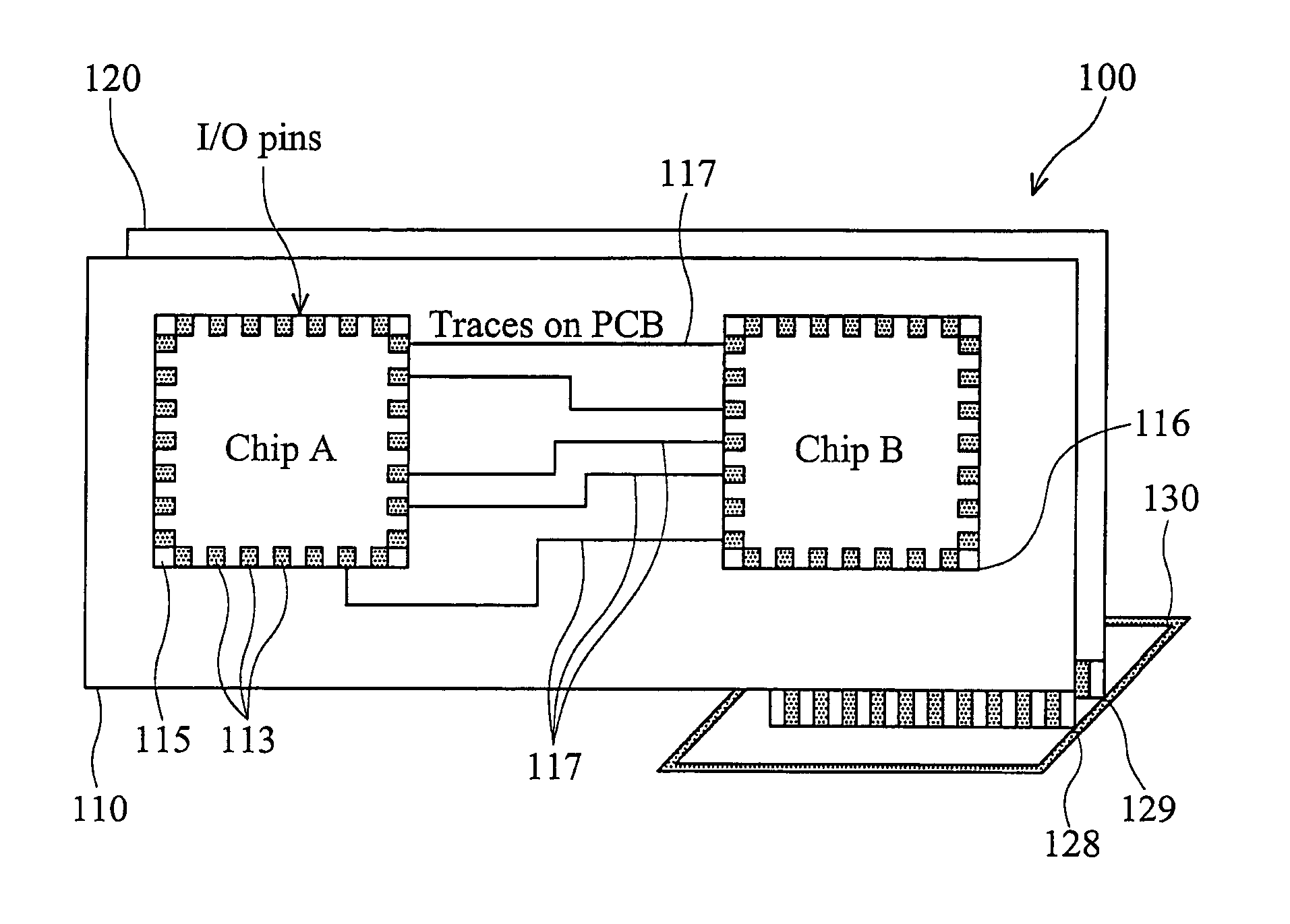
[0011]FIG. 1 is a schematic representation of a conventional inter-chip communication. Referring to FIG. 1, microelectronic package 100 is shown to include printer circuit boards (“PCB”) 110 and 120 mounted on chassis 130 through connection ports 128 and 129, respectively. PCB 110 includes chips A 115 and Chip B 116. Each of the Chip A or Chip B may include one or more microelectronic circuits integrated therein (not shown). Each of Chip A and Chip B includes a plurality of I / O pins for communicating with other electronic components. For improved efficiency, the conventional systems require that I / O pins communicate in parallel. The microelectronic circuits of Chip A communicate with the microelectronic circuits of Chip B via traces 117 f...


PUM


Abstract

In one embodiment, the disclosure relates to a method and apparatus for inter-chip wireless communication system. The system includes a first microprocessor having a plurality of non-contact ports and a first RF communication circuit integrated with the first microprocessor; a second microprocessor also having a plurality of non-contact ports and a second RF communication circuit integrated therein. An RF communication protocol can be configured to receive data from each of the non-contact ports in parallel, multiplex and translate the data to a serial RF signal. Data communication can be accomplished using the wireless communication circuit on each chip. The RF communication between the first and the second integrated circuits using the communication protocol defines a non capacitive-coupling of the first and the second die.

Description

BACKGROUND[0001]Semiconductor device geometries have dramatically decreased in size since such devices were first introduced several decades ago. Since then, integrated circuits have generally followed the two year / half-size rule (often called Moore's Law), which means that the number of devices on a chip doubles every two years. Today's fabrication plants are routinely producing devices having 0.35 μm and even 90 nm feature sizes. Fabrication of electronics devices typically entails designing components defined by a multitude of microelectronic circuits. Using fabrication technology, several microcircuits can be integrated on a single chip to form an integrated circuit (“IC”). The chips communicate with each other through a plurality of nodes or I / O (input / output) ports. As the integrated circuits diminish in size, new challenges arise in packaging the integrated circuit into an electronic device.[0002]Conventionally, microprocessors formed on different semiconductors communicate t...

Claims


Application Information

Patent Timeline
Patent Type & Authority Patents(United States)
IPC IPC(8): H04B1/40
CPCH04B1/38
Inventor CHEN, KER-MINHUNG, TSUNG-YANG
Owner TAIWAN SEMICON MFG CO LTD
Why Eureka
Try Eureka