Capacitance type semiconductor sensor

a semiconductor sensor and capacitance technology, applied in the direction of instruments, turn-sensitive devices, basic electric elements, etc., can solve problems such as unfavorable, and achieve the effect of excellently preventing parasitic capacitance, excellently balanced holding force, and sufficient absolute value of parasitic capacitan

Inactive Publication Date: 2008-03-04
DENSO CORP
View PDF9 Cites 7 Cited by
  • Summary
  • Abstract
  • Description
  • Claims
  • Application Information

AI Technical Summary

Benefits of technology

[0016]The present invention has been implemented in view of the foregoing situation, and has an object to prevent an adverse effect of parasitic capacitance occurring between bonding wires for electrically connecting a sensor chip and a circuit chip in a capacitance type semiconductor sensor having a stack structure in which the sensor chip is mounted on the circuit chip through adhesive film, thereby enhancing the characteristic of the capacitance type semiconductor sensor.
[0019]Furthermore, the plural bonding wires are not provided so as to be concentrated on one side portion of the sensor chip, but arranged dispersively, so that the interval between the bonding wires is increased and thus the absolute value of parasitic capacitance occurring can be reduced. Accordingly, even when the bonding wires are deformed and the parasitic capacitance between the bonding wires is varied, the variation can be suppressed to an extremely small value, and thus the effect on the sensor characteristic (detection precision) can be reduced. As a result, according to the first aspect, the adverse effect of the parasitic capacitance occurring between the bonding wires can be prevented, and the characteristic can be enhanced.
[0021]Accordingly, the interval between the four bonding wires can be sufficiently increased, and the absolute value of the parasitic capacitance can be sufficiently reduced. In addition, the adverse effect of the parasitic capacitance can be excellently prevented. In this case, the four bonding wires are kept to be pitched in four directions, and thus the sensor chip can achieve an excellently balanced holding force to the circuit chip by the bonding wires, so that an effect of enhancing the resistance to shock (preventing resonance) can be expected.
[0022]The circuit chip is mounted on the board, and electrically connected by the plural bonding wires. In this case, according to a fourth aspect, each of four bonding wires of these bonding wires may be arranged at each corner portion of the circuit chip. According to the fourth aspect, the circuit chip can achieve an excellently balanced holding force to the board by the bonding wires pitched in the four directions, so that the resonance of the circuit chip to the board can be prevented, and furthermore the effect of suppressing the shock to the sensor chip can be expected.

Problems solved by technology

Such a stress breaks the adhesion between the circuit chip 2 and the sensor chip 1, causes breaking of the bonding wires 5, etc., and thus it is not favorable.

Method used


Image

  • Capacitance type semiconductor sensor
  • Capacitance type semiconductor sensor
  • Capacitance type semiconductor sensor

Examples


first embodiment

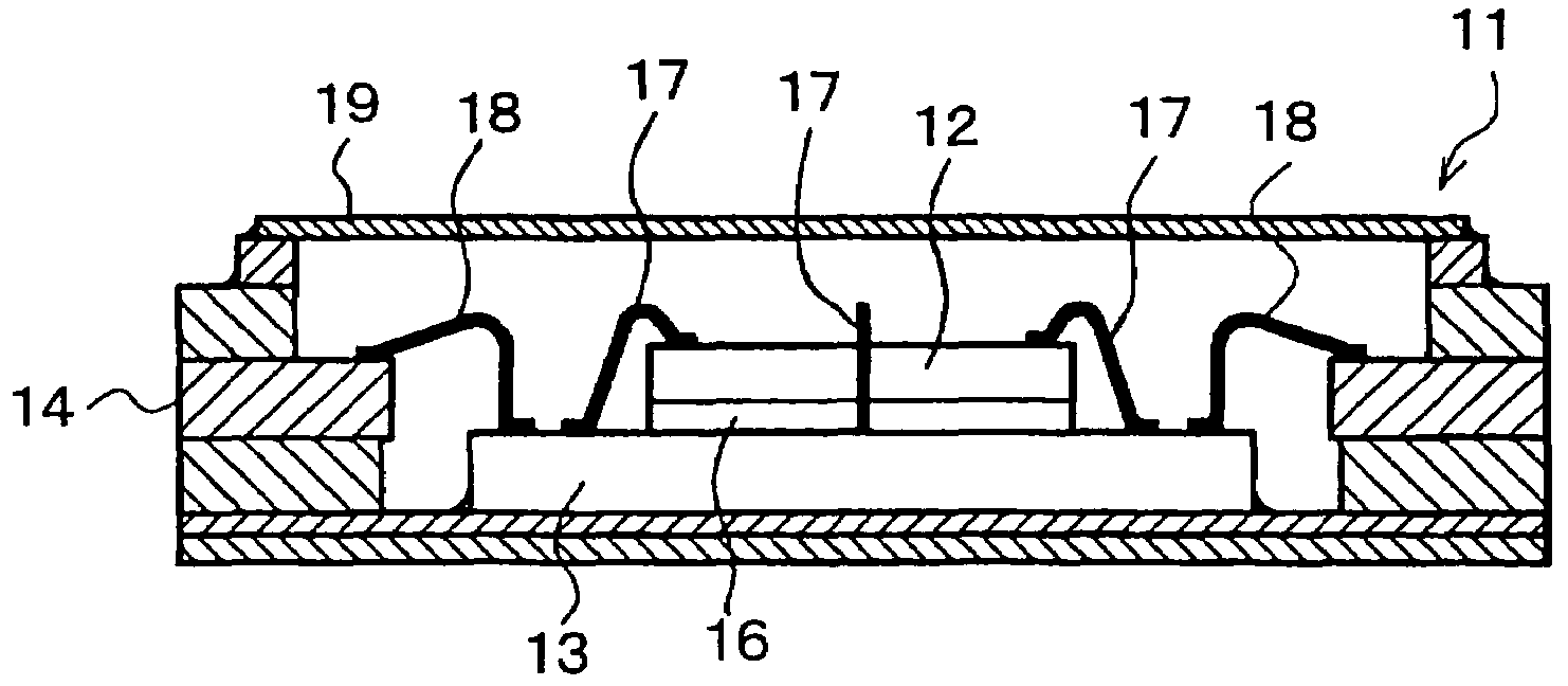
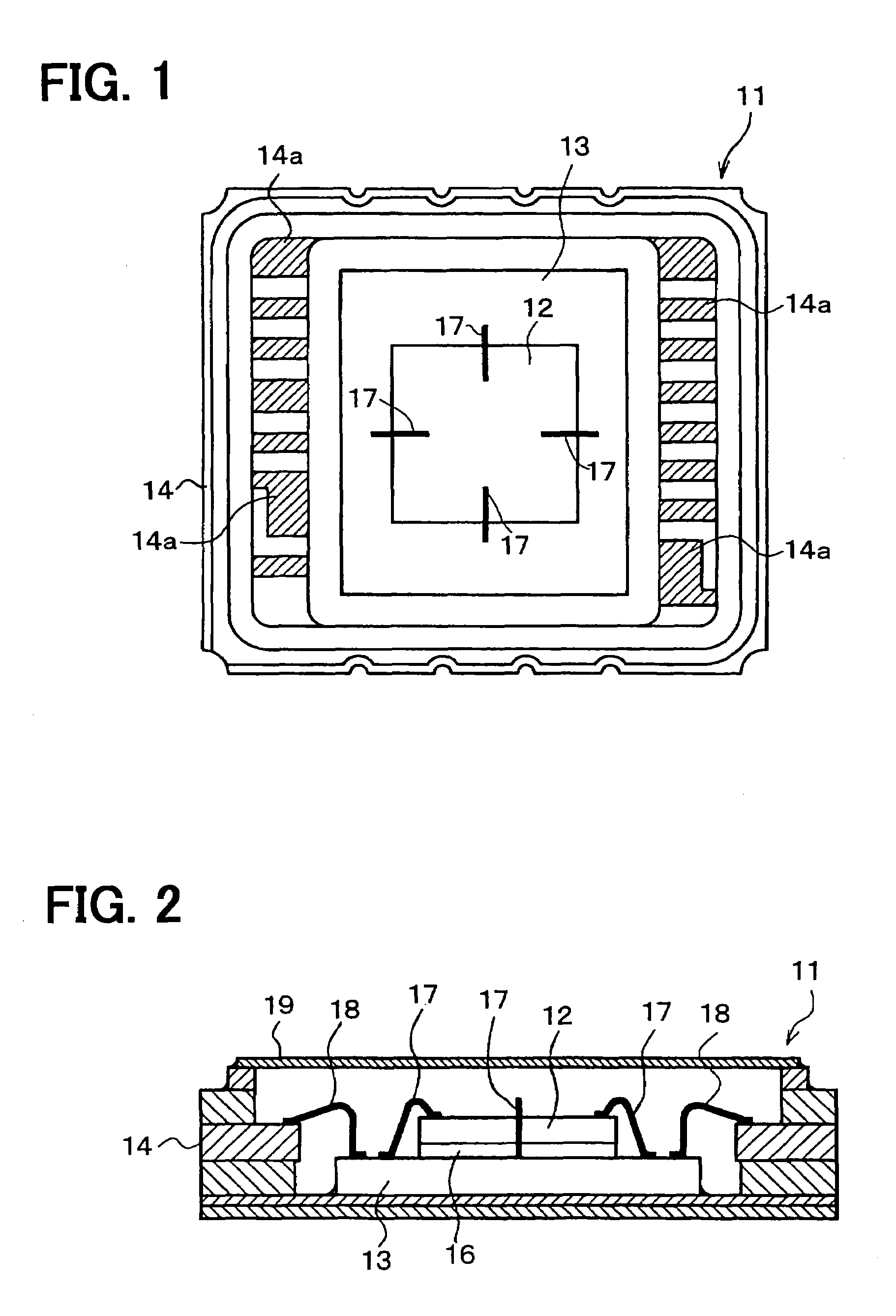
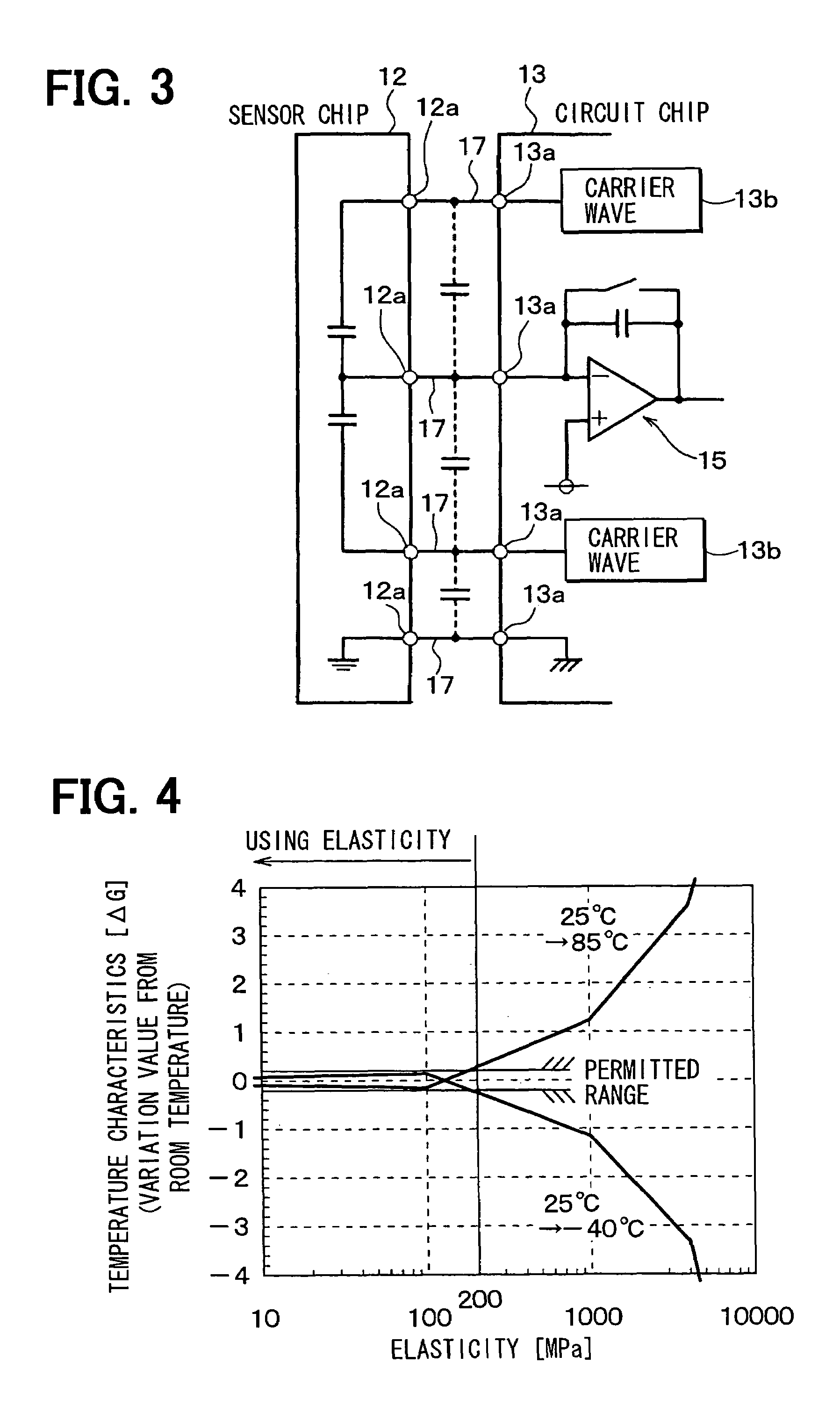
[0034]FIG. 1 is a schematic plan view showing the overall construction of an acceleration sensor as a capacitance type semiconductor sensor to which an embodiment of the present invention is applied. FIG. 2 is a longitudinally-sectional front view showing the semiconductor acceleration sensor as shown in FIG. 1, and FIG. 3 shows a part of a sensor circuit provided to the acceleration sensor. The acceleration sensor according to this embodiment will be described hereunder with reference to the drawings.

[0035]As shown in FIGS. 1 and 2, the acceleration sensor 11 of this embodiment is designed to have a stack structure in which a sensor chip 12 is mounted on a circuit chip 13, and the sensor chip 12 and the circuit chip 13 thus stacked is accommodated in a package 14 as a board. Not illustrated specifically, the sensor chip 12 is designed to be located at the center portion on the surface of a semiconductor (silicon) substrate and form an acceleration detector as a dynamic quantity det...

second embodiment

[0052]FIG. 5 shows the construction of an acceleration sensor 21 according to a second embodiment. The second embodiment is different from the first embodiment in that the four bonding wires 22 for connecting the sensor chip 12 and the circuit chip 13 are arranged so that each of the bonding wires is disposed at each of the four corner portions of the sensor chip 12.

[0053]With this construction, the interval between the four bonding wires 22 can be sufficiently increased as in the case of the first embodiment, and the absolute value of the parasitic capacitance can be sufficiently reduced. Furthermore, there can be achieved an excellent effect of preventing the adverse effect caused by the parasitic capacitance, and the characteristic can be enhanced. In addition, the four bonding wires 22 are set to be pitched in the four directions, and thus there can be achieved an effect that the excellently balanced holding force of the sensor chip 12 to the circuit chip 13 can be achieved by t...

third embodiment

[0054]FIG. 6 shows the construction of an acceleration sensor 31 according to a third embodiment. In the third embodiment, the four bonding wires 17 for connecting the sensor chip 12 and the circuit chip 13 are arranged so that each bonding wire 17 is located at the center portion of each side portion of the sensor chip 12 as in the case of the first embodiment, and in addition, (substrate) bonding wires 32 for electrically connecting the circuit chip 13 and the package 14 are arranged so that each of four bonding wires 32 thereof is located at each corner portion of the circuit chip 13.

[0055]According to this embodiment, the same effect as the first embodiment can be achieved, and also the excellently balanced holding force-of the circuit chip 13 to the package 14 can be achieved by the substrate bonding wires 32 which are kept to be pitched in the four directions, and consequently it is expected that the resonance of the circuit chip 13 to the package 14 can be prevented, and furt...


PUM


Abstract

In a capacitance type semiconductor dynamic quantity sensor, a sensor chip and a circuit are connected to each other through adhesive film having an elasticity of 200 MPa or less to reduce the temperature characteristic. Four bonding wires for connecting the sensor chip and the circuit chip are arranged so that each of the bonding wires is located at the center portion of each side portion of the sensor chip or at each corner portion of the sensor chip, thereby sufficiently increasing the interval between the bonding wires and thus sufficiently reducing the absolute value of the parasitic capacitance thus occurring. Therefore, even when the parasitic capacitance between the four bonding wires is varied, the variation is very small, and thus the influence on the sensor characteristic can be reduced.

Description

CROSS REFERENCE TO RELATED APPLICATION[0001]This application is based upon, claims the benefit of priority of, and incorporates by reference the contents of, Japanese Patent Application No. 2004-260742 filed on Sep. 8, 2004.FIELD OF THE INVENTION[0002]The present invention relates to a capacitance type semiconductor sensor for detecting a dynamic quantity of an acceleration sensor, a gyro sensor or the like as a variation of electrostatic capacitance.BACKGROUND OF THE INVENTION[0003]A device having a stack structure in which semiconductor chips are stacked as shown in FIGS. 7 and 8 (for example, see JP-A-2000-227439) is known as one of the capacitance type semiconductor sensors as described above, for example, as a semiconductor acceleration sensor for an air bag of a vehicle, for example. According to this device, a sensor chip 1 having an acceleration detector is adhesively mounted on a circuit chip 2 having a signal processing circuit and further the circuit chip 2 is adhesively ...

Claims


Application Information

Patent Timeline
Patent Type & Authority Patents(United States)
IPC IPC(8): H01L23/48H01L23/52G01C19/56G01C19/5769G01P15/125H01L29/84
CPCG01P1/023G01P15/125H01L2224/32145H01L2224/48091H01L2924/01078H01L2924/00014H01L2924/01068
Inventor KITAO, NORIOUMEMURA, AKINOBU
Owner DENSO CORP
Why Eureka
Try Eureka