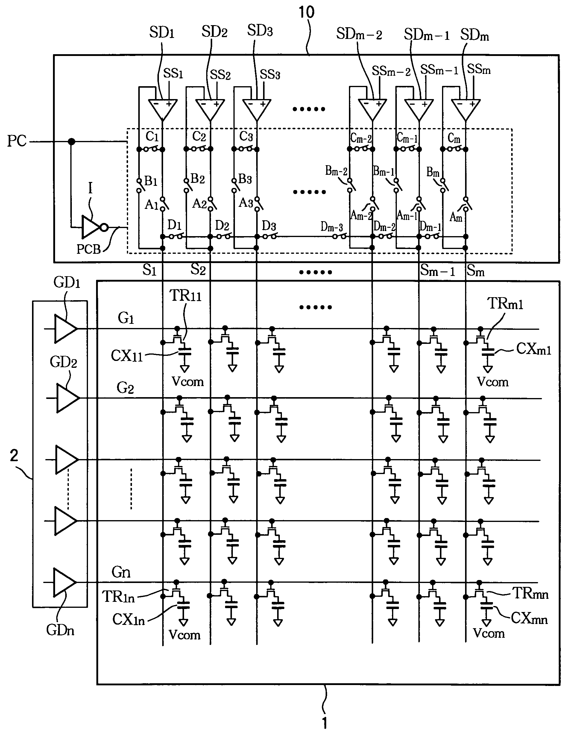
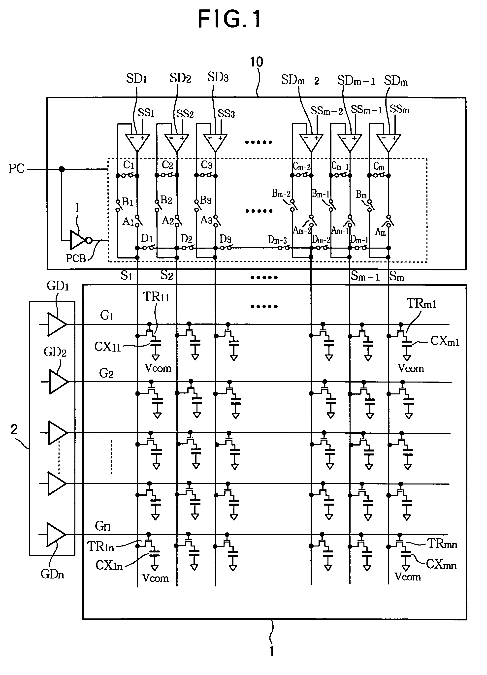
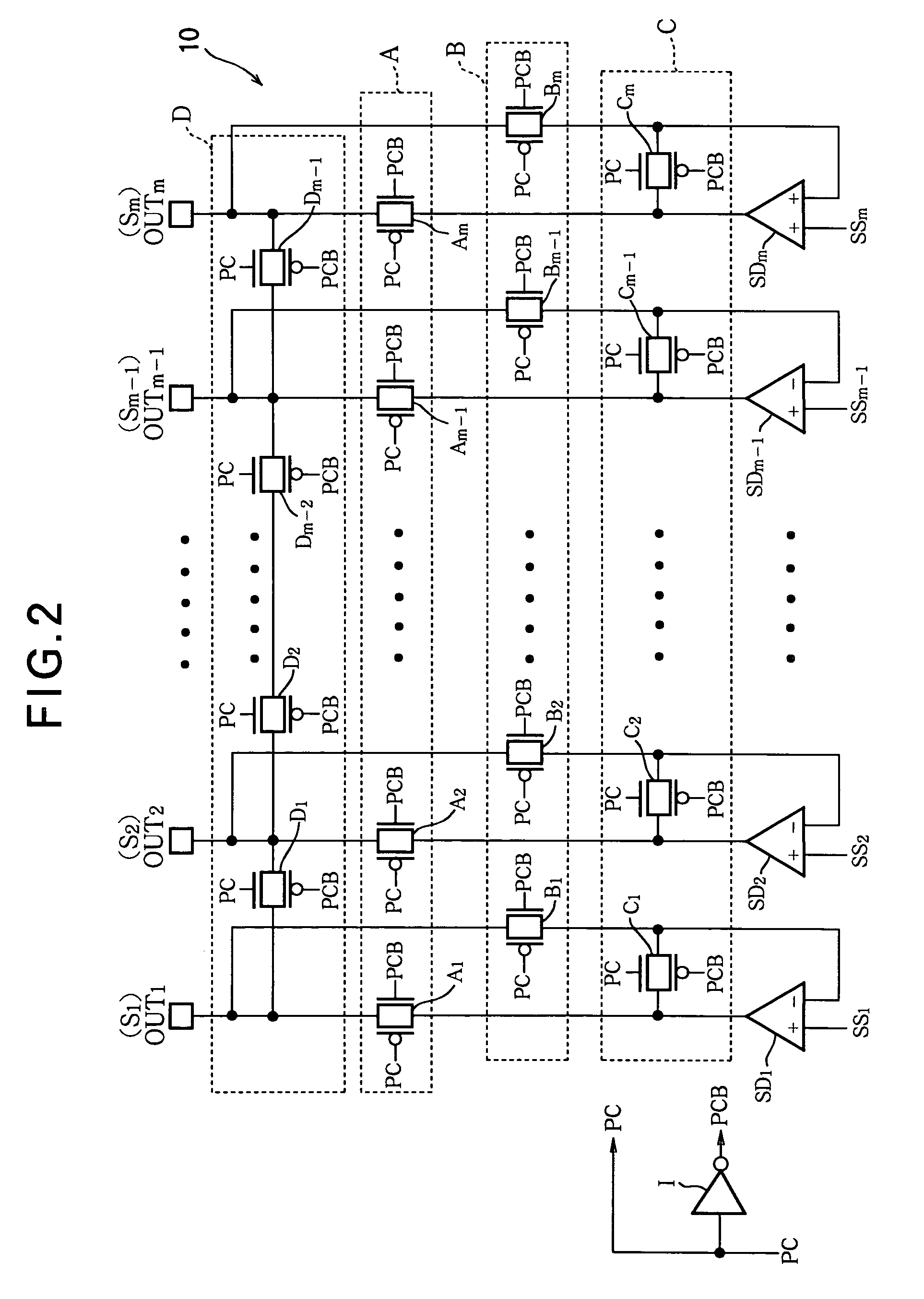
Output circuit, liquid crystal driving circuit, and liquid crystal driving method
a technology of output circuit and liquid crystal, applied in the direction of instruments, static indicating devices, etc., can solve the problems of reducing image quality, limiting the speed with which the liquid crystal panel can be driven, and impairing accuracy, so as to achieve quick and accurate adjustment of output speed and high speed
- Summary
- Abstract
- Description
- Claims
- Application Information
AI Technical Summary
Benefits of technology
Problems solved by technology
Method used
Image
Examples
second embodiment
[0055]Referring to FIG. 5, the source driving circuit 20 in the second embodiment comprises m source drivers SD1, SD2, . . . , SDm, an A-group of analog switches that control output paths, a B-group of analog switches that control first feedback paths, a C-group of analog switches that control second feedback paths, an E-group of analog switches that control precharging, an a-group of protective resistors, a b-group of feedback resistors, a group of m output terminals OUT1, OUT2, . . . , OUTm, and an inverter I, where m is an even number.
[0056]The source driving circuit 20 accordingly adds protective resistors and feedback resistors to the source driving circuit 10 in the first embodiment, and alters the group of analog switches that control precharging. The source driving circuit 20 in the second embodiment also arranges the feedback paths during the driving period so that they branch from points following the protective resistors.
[0057]The E-group of analog switches comprises m / 2 ...
third embodiment
[0078]Referring to FIG. 6, the source driving circuit 30 in the third embodiment comprises m source drivers SD1, SD2, . . . , SDm, an A-group of analog switches that control output paths, a B-group of analog switches that control first feedback paths, a C-group of analog switches that control second feedback paths, an F-group of analog switches that control precharging, a group of m output terminals OUT1, OUT2, . . . , OUTm, and an inverter I, where m is an arbitrary integer equal to or greater than two.
[0079]The source driving circuit 30 in the third embodiment accordingly alters the group of analog switches that control precharging in the source driving circuit 10 (see FIGS. 1 and 2) in the first embodiment.
[0080]The F-group of analog switches comprises m analog switches (MOS switches) F1, F2, . . . , Fm. Analog switch Fi is connected between the i-th output terminal OUTi (source line Si) of the source driving circuit 30 and the common voltage Vcom (the potential of the common ele...
PUM
| Property | Measurement | Unit |
|---|---|---|
| power | aaaaa | aaaaa |
| impedance | aaaaa | aaaaa |
| driving speed | aaaaa | aaaaa |
Abstract
Description
Claims
Application Information


