MEMS sensor suite on a chip

a sensor suite and chip technology, applied in the field of environmental sensors, can solve the problems of occupying a lot of space, and individual packages are difficult to integrate the sensing functions of temperature sensors, humidity sensors, accelerometers, etc., and achieves the effect of integrating the two sensing functions of accelerometers and humidity sensors much more difficult, and limiting the miniaturization of the sensor sui

Active Publication Date: 2008-05-06
MORGAN RES CORP
View PDF1 Cites 31 Cited by
  • Summary
  • Abstract
  • Description
  • Claims
  • Application Information

AI Technical Summary

Problems solved by technology

However, this approach limits the miniaturization of the sensor suite.
The individual packages take up a lot of space, as do the relatively large circuit traces on a printed circuit board.
However, integrating all three sensing functions of accelerometers, temperature sensors, and humidity sensors (or integrating the two sensing functions of accelerometers and humidity sensors) is much more difficult.
Integration challenges lie in the sensor design, sensor fabrication, and sensor packaging.
The challenges are due to the sensor devices having substantially different functionality.
Integrating exposed sensors and sensors that should not be exposed is difficult from a packaging perspective.

Method used


Image

  • MEMS sensor suite on a chip
  • MEMS sensor suite on a chip
  • MEMS sensor suite on a chip

Examples


Embodiment Construction

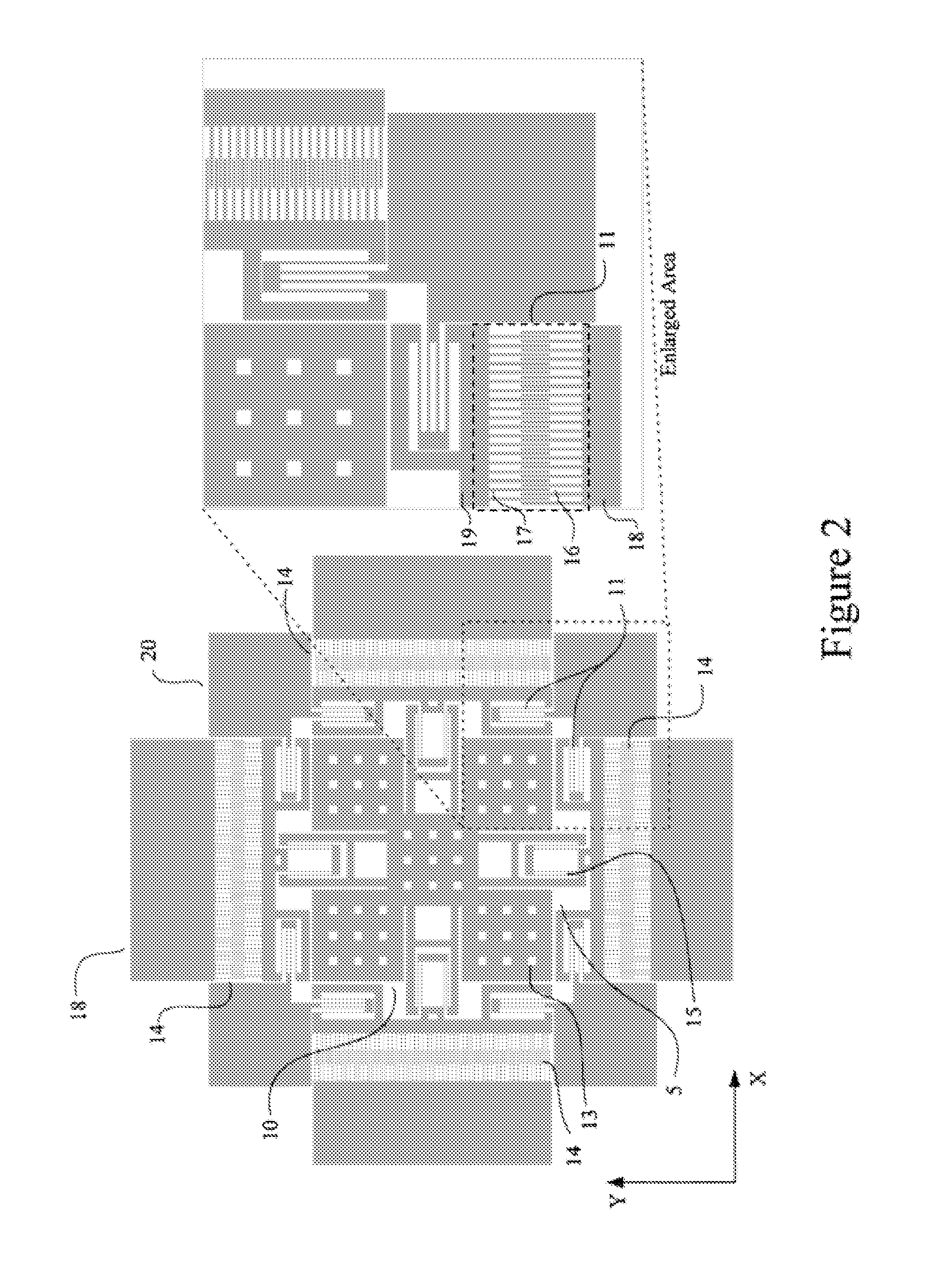
[0024]The present invention and its advantages are best understood by referring to the drawings. The elements of the drawings are not necessarily to scale, emphasis instead being placed upon clearly illustrating the principles of the invention.

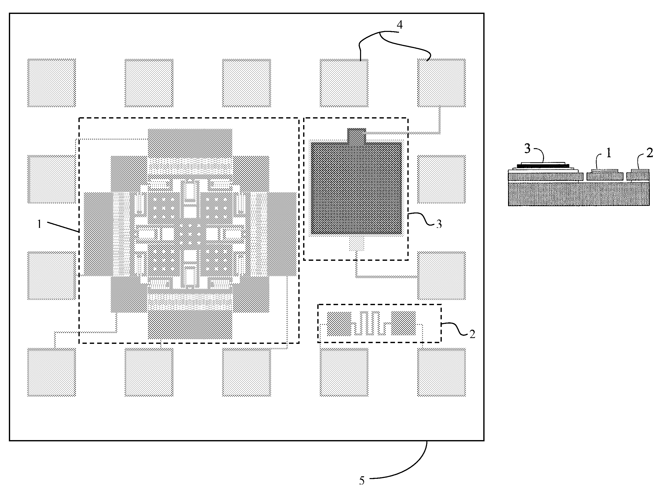
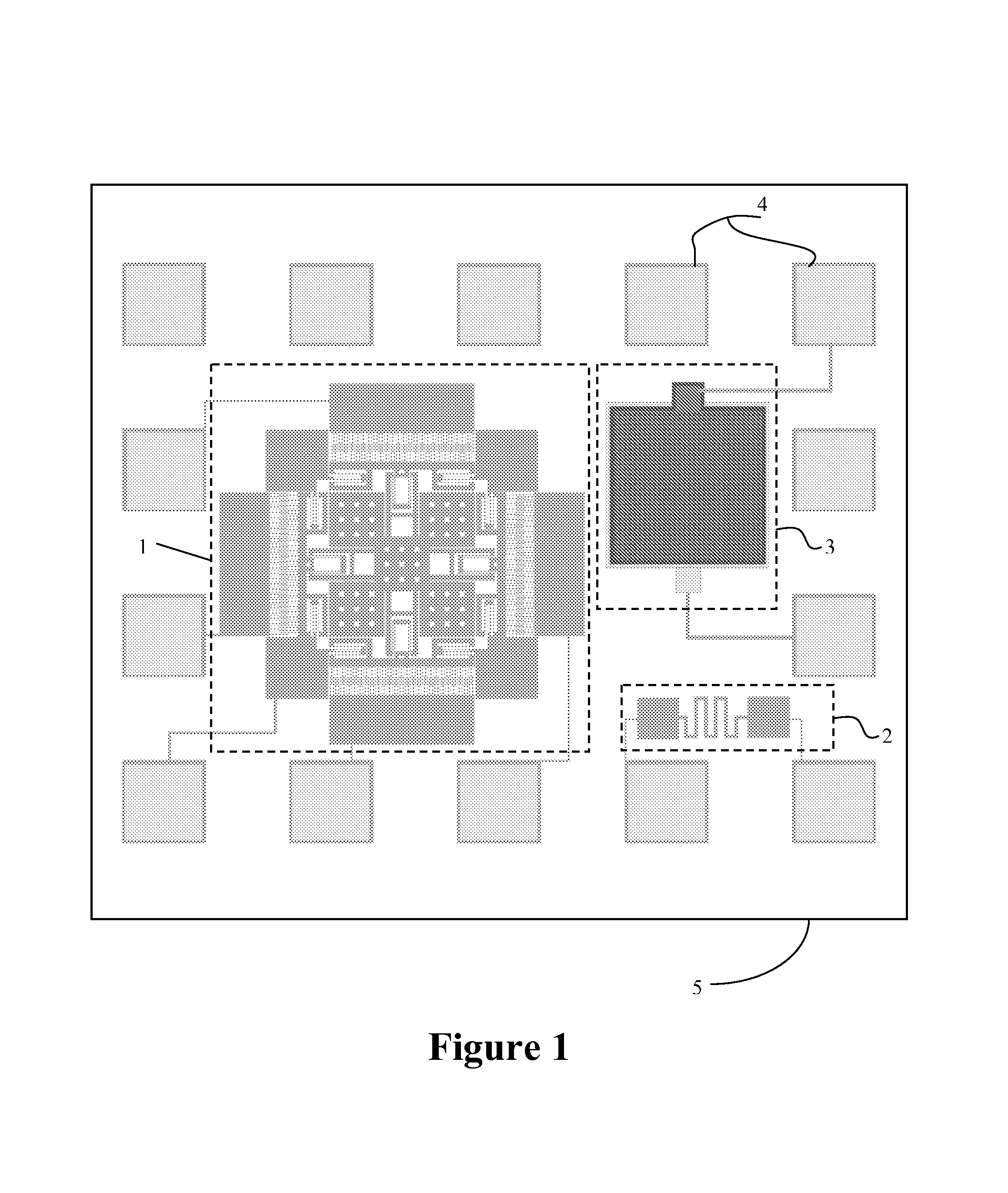
[0025]The illustrated embodiment of the invention is fabricated in a thick layer of silicon or other conductor material. Within this thick layer of material, the proof masses, flexures, capacitive position sensors, isolated resistors, humidity sensitive capacitors, and multiple anchors and pads are fabricated. FIG. 1 shows one configuration of these structures that yields a sensor suite with a two-axis accelerometer 1, a temperature sensor 2, and a humidity sensor 3. The three sensors occupy an area on the substrate surface 5 of about 0.5 square centimeters or less. Bonding pads 4 provide electrical connection to the three sensors.

The Accelerometer

[0026]FIG. 2 shows one embodiment of the device's accelerometer, in which a moveable proof mass 1...


PUM


Abstract

The MEMS Sensor Suite on a Chip provides the capability, monolithically integrated onto one MEMS chip, to sense temperature, humidity, and two axes of acceleration. The device incorporates a MEMS accelerometer, a MEMS humidity sensor, and a MEMS temperature sensor on one chip. These individual devices incorporate proof masses, suspensions, humidity sensitive capacitors, and temperature sensitive resistors (thermistors) all fabricated in a common fabrication process that allows them to be integrated onto one micromachined chip. The device can be fabricated in a simple micromachining process that allows its size to be miniaturized for embedded and portable applications. During operation, the sensor suite chip monitors temperature levels, humidity levels, and acceleration levels in two axes. External circuitry allows sensor readout, range selection, and signal processing.

Description

REFERENCE TO RELATED APPLICATIONS[0001]This application claims priority to Provisional Patent Application U.S. Ser. No. 60 / 619,421, entitled “MEMS Sensor Suite on a Chip” and filed on Oct. 15, 2004, which is fully incorporated herein by reference.GOVERNMENT LICENSE RIGHTS[0002]This invention was made with Government support under contract number DAAE30-03-C-1076, awarded by the United States Army. The Government has certain rights in the invention.BACKGROUND[0003]1. Field of the Invention[0004]The present invention relates generally to environmental sensors. More particularly, the present invention relates to micro-electromechanical (“MEMS”) humidity sensors, accelerometers, and resistors.[0005]2. Background of the Invention[0006]Embedding miniature sensors in structures, systems, storage and shipping containers, and other items allows the monitoring of those items to determine health, maintenance needs, lifetime, and other item characteristics. In addition, embedded sensors can be ...

Claims


Application Information

Patent Timeline
Patent Type & Authority Patents(United States)
IPC IPC(8): H01L21/00
CPCB81C1/00246B81B2201/0235B81B2201/0278B81B2201/0292G01P2015/082G01P2015/084G01P2015/0842
Inventor KRANZ, MICHAEL SCOTTELLIOTT, ROBERT FAYEWHITLEY, MICHAEL RAYWILLIAMS, MARTY RAYREINER, PHILIP JOHN
Owner MORGAN RES CORP
Why Eureka
Try Eureka