Low power bipolar transistors with low parasitic losses

Inactive Publication Date: 2008-05-13
HRL LAB
View PDF6 Cites 5 Cited by
  • Summary
  • Abstract
  • Description
  • Claims
  • Application Information

AI Technical Summary

Benefits of technology

[0006]The invention relates to a low power double heterojunction bipolar transistor (DHBT), and methods for making the same. The low power heterojunction bipolar transistor includes a collector, a base, and a emitter. The collector, the base, and the emitter are made of Indium-Arsenide-Phosphide or InAs1−xPx (x=0 to 0.5). The presence of a narrow-gap semiconductor, such as InAs (InAs1−xPx (x=0)) whose band gap is 0.35 eV in a portion of the base layer, enables low power operation. The invention provides a transistor embodiment that is fabricated such that the collector region underneath a base contact area is deactivated. This results in a drastic reduction of the base-collector parasitic capacitance, Cbc.
[0007]One exemplary embodiment of the present invention provides a bipolar transistor that has an extrinsic base and a collector. The embodiment reduces a parasitic base-collector capacitance of the bipolar transistor by deactivating a part of the collector region that overlaps the extrinsic base.

Problems solved by technology

As such, the conventional mesa structure is not optimal for parasitics reduction due to the following disadvantage: Independent optimization of the extrinsic base contact area and the capacitance Cbc is not possible.
Additionally, the base contact area cannot be increased without incurring a capacitance Cbc penalty.

Method used


Image

  • Low power bipolar transistors with low parasitic losses
  • Low power bipolar transistors with low parasitic losses
  • Low power bipolar transistors with low parasitic losses

Examples


Embodiment Construction

[0045]The invention is described below, with reference to detailed illustrative embodiments. It will be apparent that the invention can be embodied in a wide variety of forms, some of which may be quite different from those of the disclosed embodiments. Consequently, the specific structural and functional details disclosed herein are merely representative and do not limit the scope of the invention.

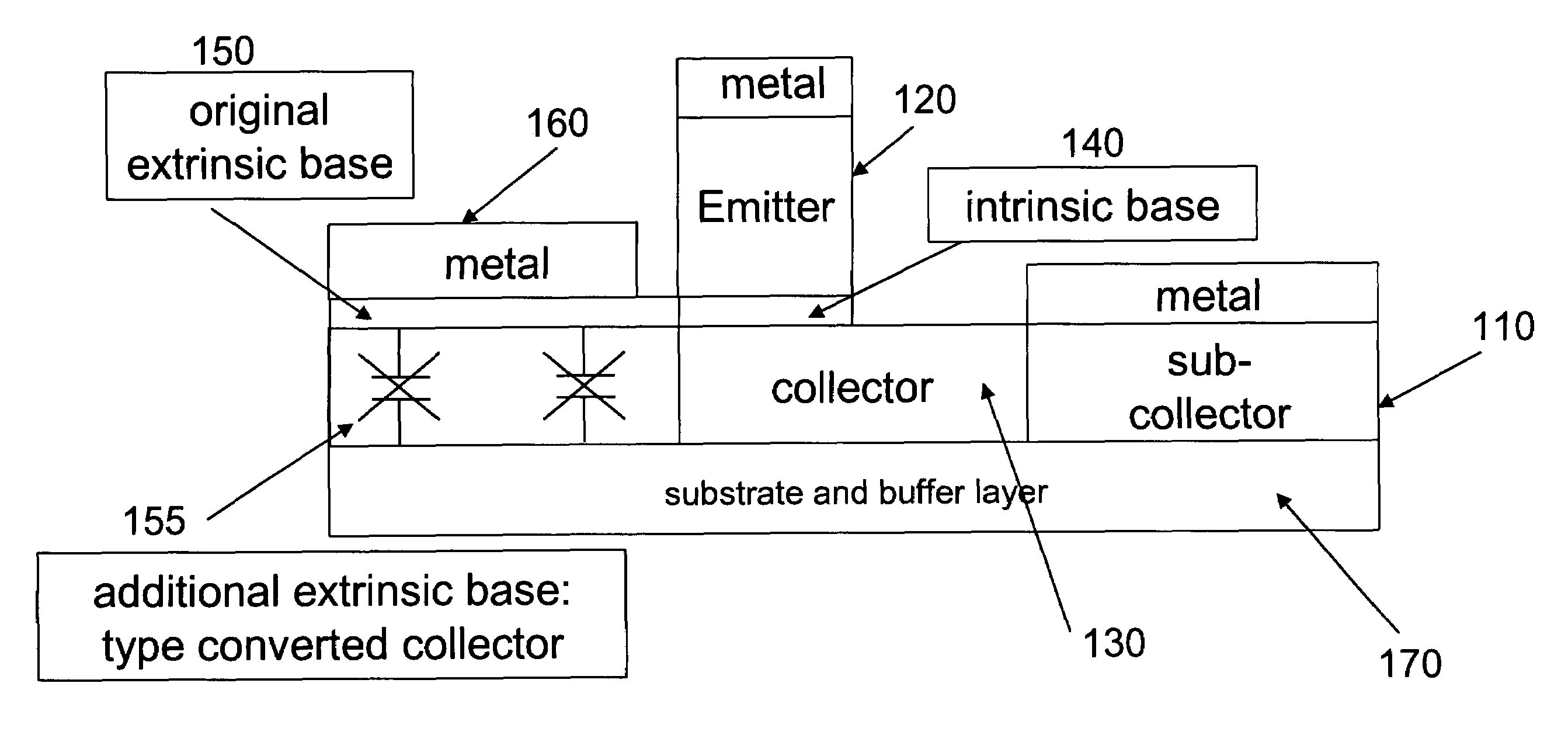
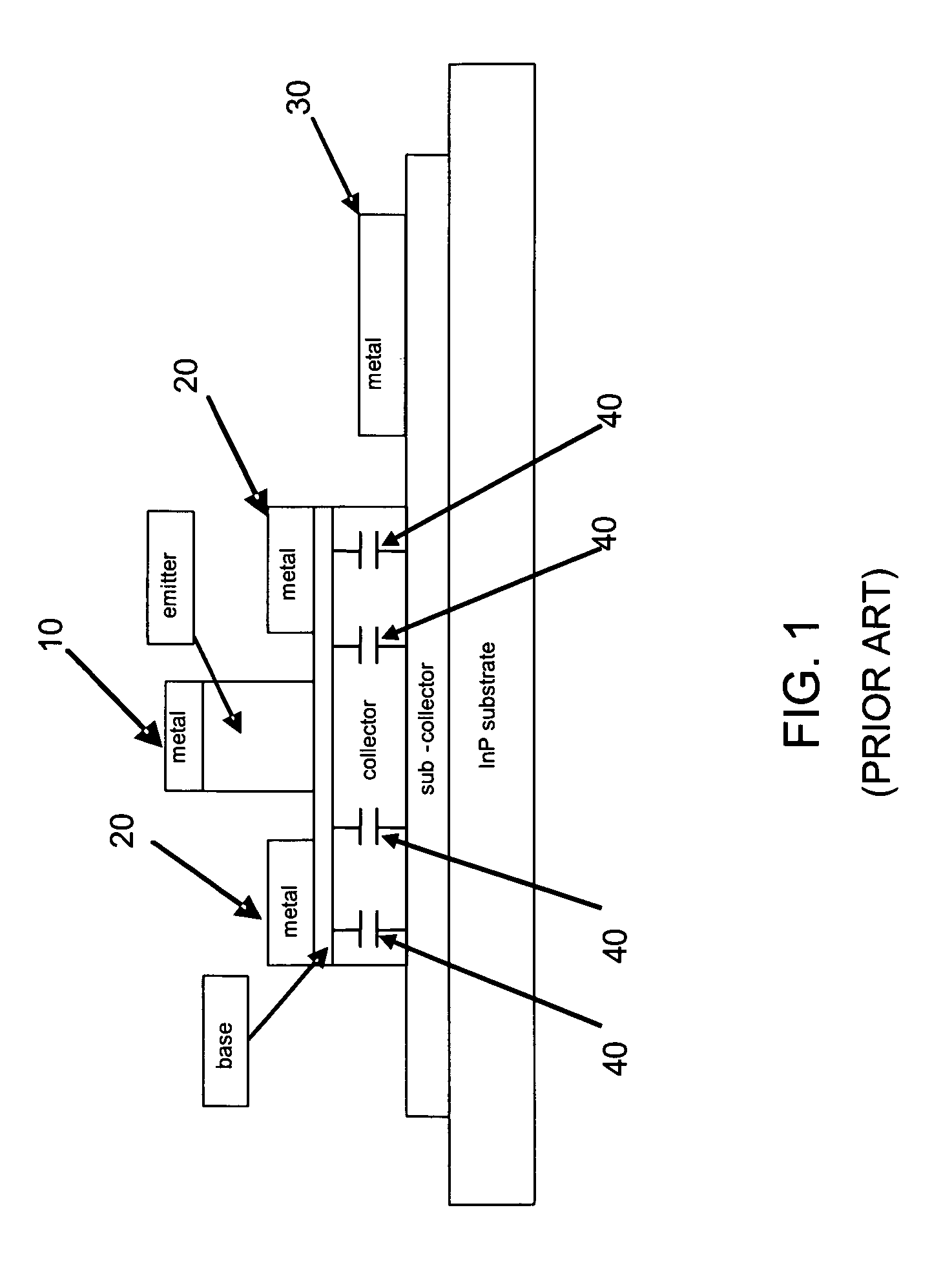
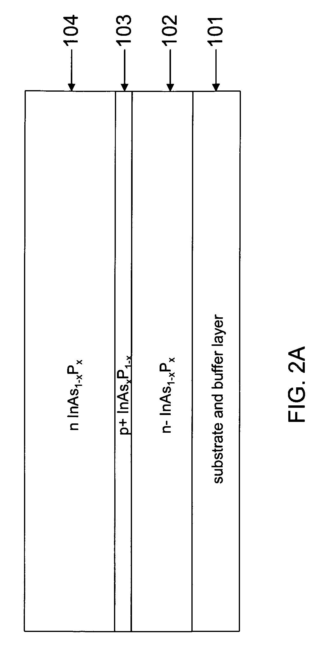
[0046]The invention relates to bipolar junction transistors (BJTs) and heterojunction bipolar transistors (HBTs) and methods for making the same. HBTs with architectures that enable the independent optimization of extrinsic base resistance and base-collector capacitance Cbc are highly desirable. An embodiment of the present invention provides a transistor architecture for which the base contact area can be decoupled from the collector and hence allows for dramatic reduction in the parasitics of transistors. A transistor in one embodiment of the present invention uses a selectively doped s...


PUM


Abstract

Low power double heterojunction bipolar transistors with low parasitics, and methods for making the same is presented. A transistor is fabricated such that the collector region underneath a base contact area is deactivated. This results in a drastic reduction of the base-collector parasitic capacitance, Cbc. An embodiment of the present invention provides a transistor architecture for which the base contact area can be decoupled from the collector and hence allows for dramatic reduction in the parasitics of transistors.

Description

STATEMENT REGARDING FEDERALLY SPONSORED RESEARCH OR DEVELOPMENT[0001]This invention was made with U.S. Government support under Contract No. N66001-01-C08033 awarded by the Defense Advanced Research Projects Agency through the Space and Naval Warfare Systems Command (DARPA / SPAWAR). The U.S. Government has certain rights to this invention.FIELD OF THE INVENTION[0002]The invention relates generally to bipolar junction transistors (BJTs) and methods for making the same. More particularly, the invention relates to low power bipolar transistors with low parasitic losses and methods for making the same.BACKGROUND OF THE INVENTION[0003]Typically, a BJT consists of a vertical stack of npn or pnp semiconductor materials. A BJT can take the form of a double heterojunction bipolar transistor (DHBT), as compared to a homojunction BJT. High speed operation is achieved through judicious scaling down of the thickness of the vertical stack of semiconductors and scaling down of the lateral dimension...

Claims


Application Information

Patent Timeline
IPC IPC(8): H01L29/73
CPCH01L29/1004H01L29/66318H01L29/7371
Inventor RAJAVEL, RAJESH D.ELLIOTT, KENNETHCHOW, DAVID H.
Owner HRL LAB
Why Eureka
Try Eureka