Method of utilizing a contact printing stamp

a technology of contact printing and stamps, applied in the direction of printing press parts, yarn, transportation and packaging, etc., can solve the problems of corresponding decrease in the feature size of integrated circuit devices, continued decrease in the feature size of integrated circuits, and approaching a limi

Active Publication Date: 2008-05-20
SAMSUNG ELECTRONICS CO LTD
View PDF14 Cites 90 Cited by
  • Summary
  • Abstract
  • Description
  • Claims
  • Application Information

AI Technical Summary

Problems solved by technology

In turn, this increase in complexity has driven a corresponding decrease in the feature size of integrated circuit devices, which has typically followed “Moore's Law.” However, the continued decrease in feature size of integrated circuits, into the nanometer regime, has become increasingly more difficult, and may be approaching a limit, because of a combination of physical and economic reasons.
Some of the newer higher resolution projection systems require expensive radiation sources such as synchrotrons.
Thus, direct write systems, typically, have a much lower throughput when compared to projection systems again leading to either increased complexity in manufacturing or increased cost or both.
This example of imprint lithography uses a nano-imprinting step, which has so far not been consistently and successfully used in a manufacturing process.
In addition, this example also includes lithographic materials and several processes that may limit its process capability.
This randomness along with the difficulty of physically manipulating nanometer-sized components presents a significant challenge to the fabrication of reproducible and practical nanometer-scale devices.
If these problems persist, the continued growth, seen over the past several decades, in cheaper, higher speed, higher density, and lower power integrated circuits used in electronic devices will be impractical.
The ability to optimize the formation of nanometer-scale devices, will open up a wide variety of applications that are currently either impractical or are not cost effective.

Method used


Image

  • Method of utilizing a contact printing stamp
  • Method of utilizing a contact printing stamp
  • Method of utilizing a contact printing stamp

Examples


Embodiment Construction

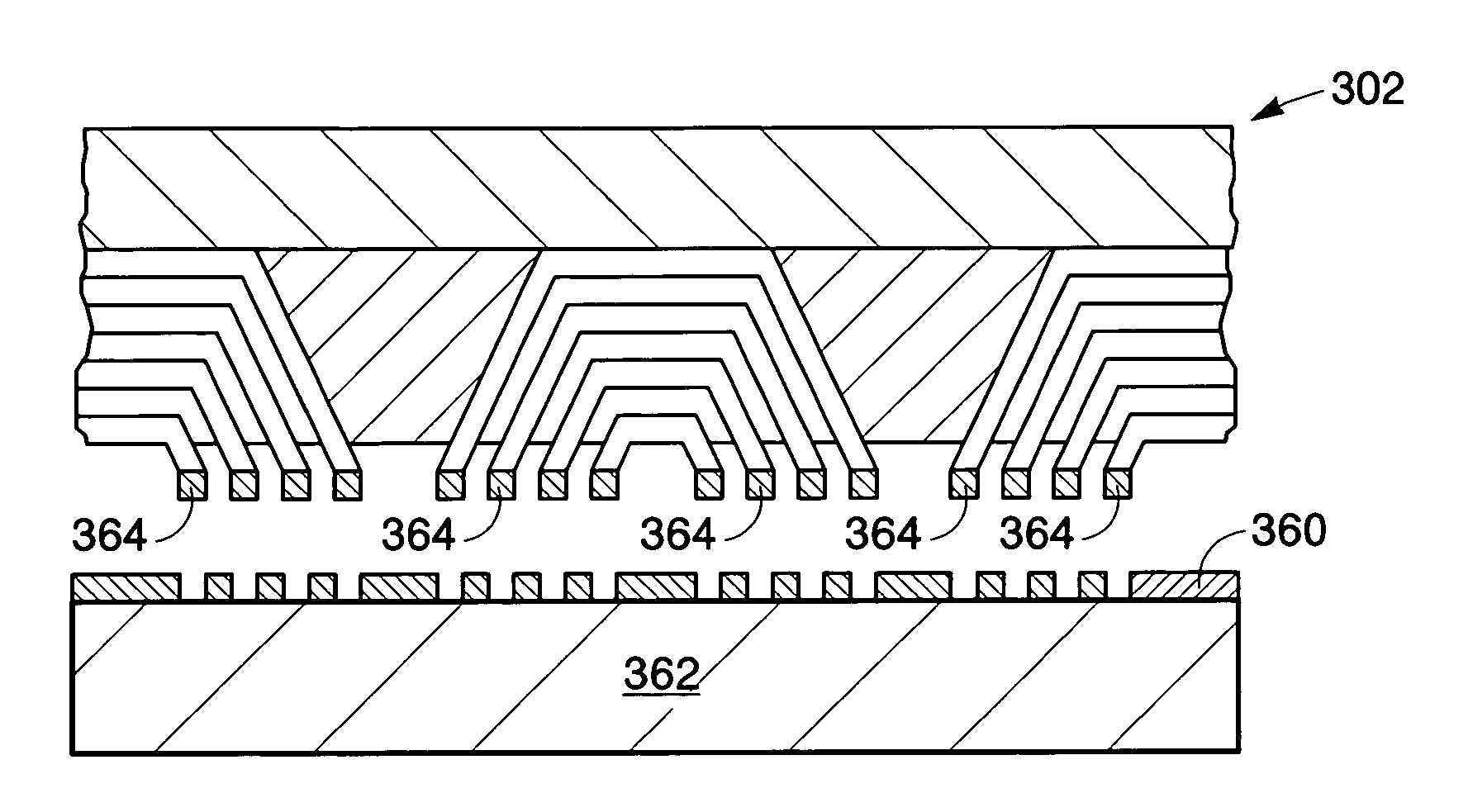
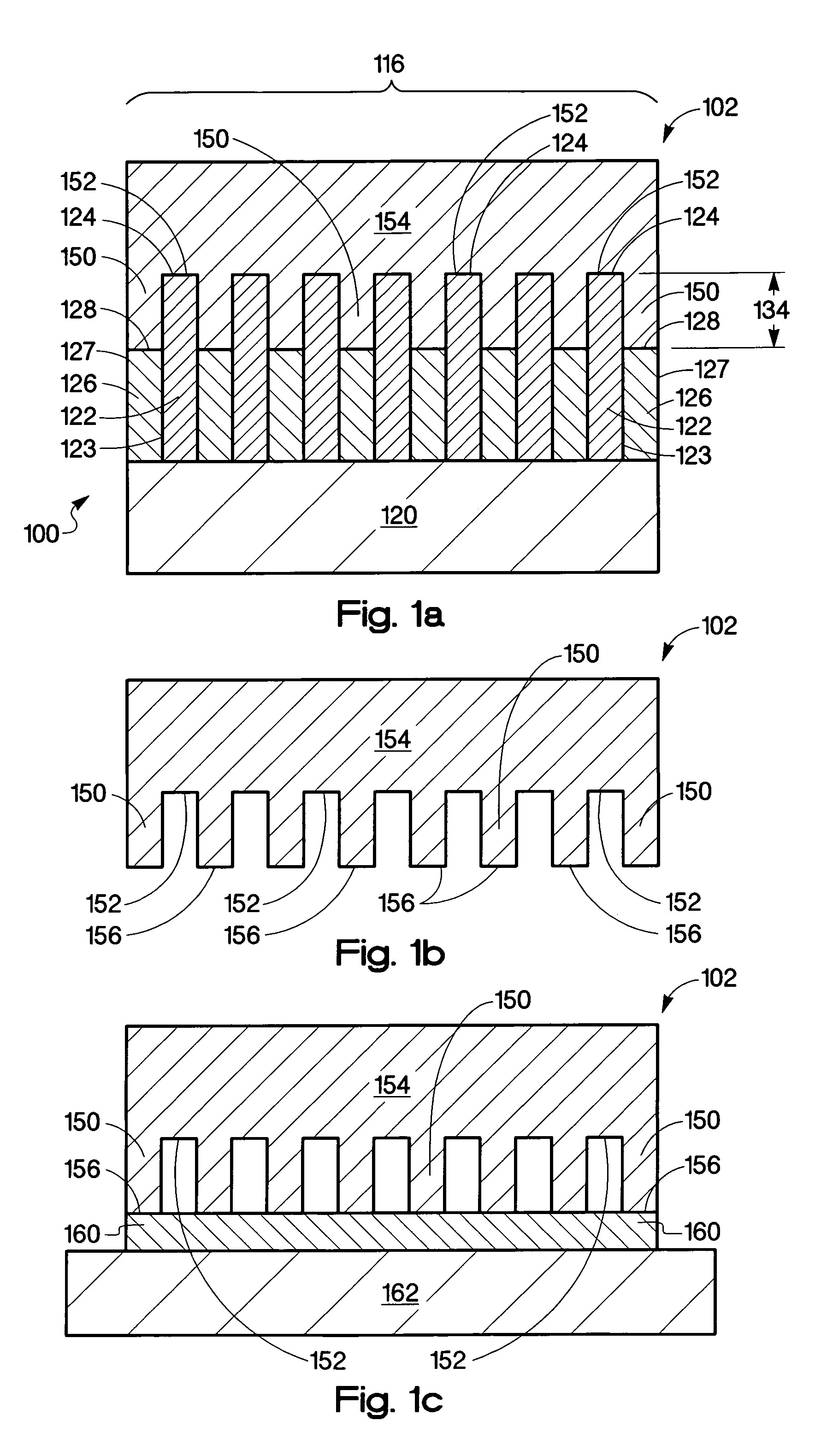
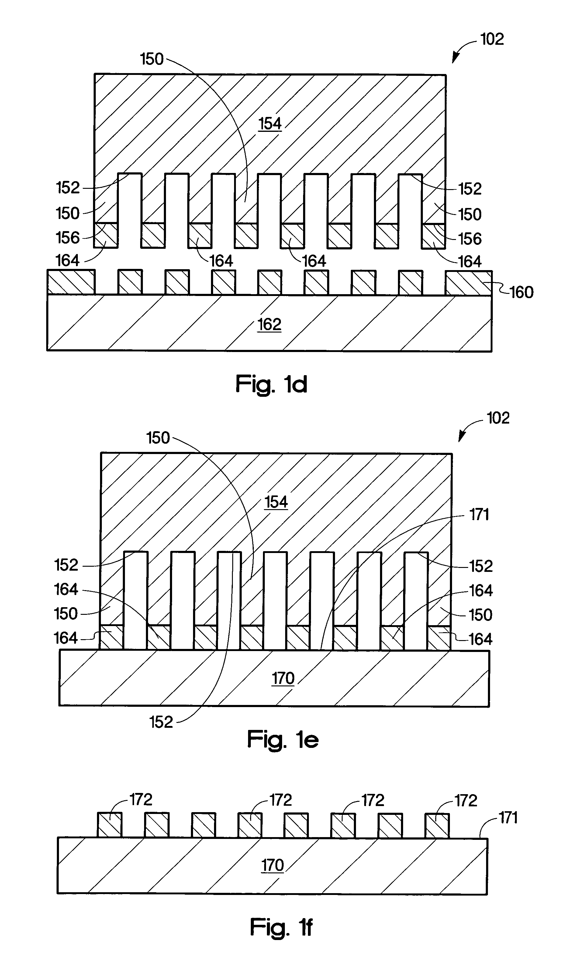
[0023]This invention is directed to utilizing a contact printing stamp created using multilayer thin film structures, sometimes referred to as superlattices, to act as the template, mold, or some combination thereof in forming the stamp. Typically, the present invention utilizes alternating layers of two dissimilar materials having differing etching or removal rates to form the master mold surfaces for generating the protrusions and indentations of the contact printing stamp. In addition, multiple materials may be utilized in the multilayer thin film structure to generate even more complex template structures. The contact printing stamp of the present invention may be fabricated by a variety of techniques and materials. The present invention enables a reduction in the characteristic feature size formed in the contact printing stamp from approximately 80 nanometers to 2 or 3 nanometers or even lower. The present invention also allows for larger features, up to microns in characterist...


PUM


Abstract

A method of using a contact printing stamp, including forming a transfer material on a plurality of stamping surfaces. The plurality of stamping surfaces are disposed on a plurality of stamp protrusions adapted from the forming of a stamp material in a plurality of recessed regions formed in an exposed end-region of a multilayer thin film structure.

Description

CROSS-REFERENCE TO RELATED APPLICATION[0001]This application is related to co-pending and commonly assigned application serial number 11 / 046,321 filed 28 Jan. 2005 by Pavel Komilovich, Peter Mardilovich, and Kevin F. Peters and entitled “Method of Forming a Contact Printing Stamp.”BACKGROUNDDescription of the Art[0002]Over the past few years, the demand for ever cheaper and lighter weight portable electronic devices has led to a growing need to manufacture durable, lightweight, and low cost electronic circuits of increasing complexity, including high density memory chips. To a large extent, over the past thirty years, this growth has been fueled by a nearly constant exponential increase in the capabilities of microelectronic devices; producing unprecedented advances in computational, telecommunication, and signal processing capabilities. In turn, this increase in complexity has driven a corresponding decrease in the feature size of integrated circuit devices, which has typically fol...

Claims


Application Information

Patent Timeline
Patent Type & Authority Patents(United States)
IPC IPC(8): H01L21/00
CPCH05K3/1275H05K2203/0108Y10T428/2936H05K2203/0338H05K2203/0113
Inventor KORNILOVICH, PAVELMARDILOVICH, PETERPETERS, KEVIN F
Owner SAMSUNG ELECTRONICS CO LTD
Why Eureka
Try Eureka