
Transformer and assembling process thereof

a technology of transformer and assembling process, which is applied in the direction of basic electric elements, coils, electrical apparatus, etc., can solve the problems of pin failure to be fixed to the system circuit board, uneven pins, and difficult manipulation of the dispensing procedure, so as to improve heat dissipation

Active Publication Date: 2008-05-20
DELTA ELECTRONICS INC
View PDF4 Cites 0 Cited by
  • Summary
  • Abstract
  • Description
  • Claims
  • Application Information

AI Technical Summary

Benefits of technology

[0007]It is an object of the present invention to provide a transformer and a process of assembling the transformer by introducing an interface layer to position the circuit board and enhance heat dissipation.
[0010]It is another object of the present invention to provide a transformer having simplified assembling process and structure.

Problems solved by technology

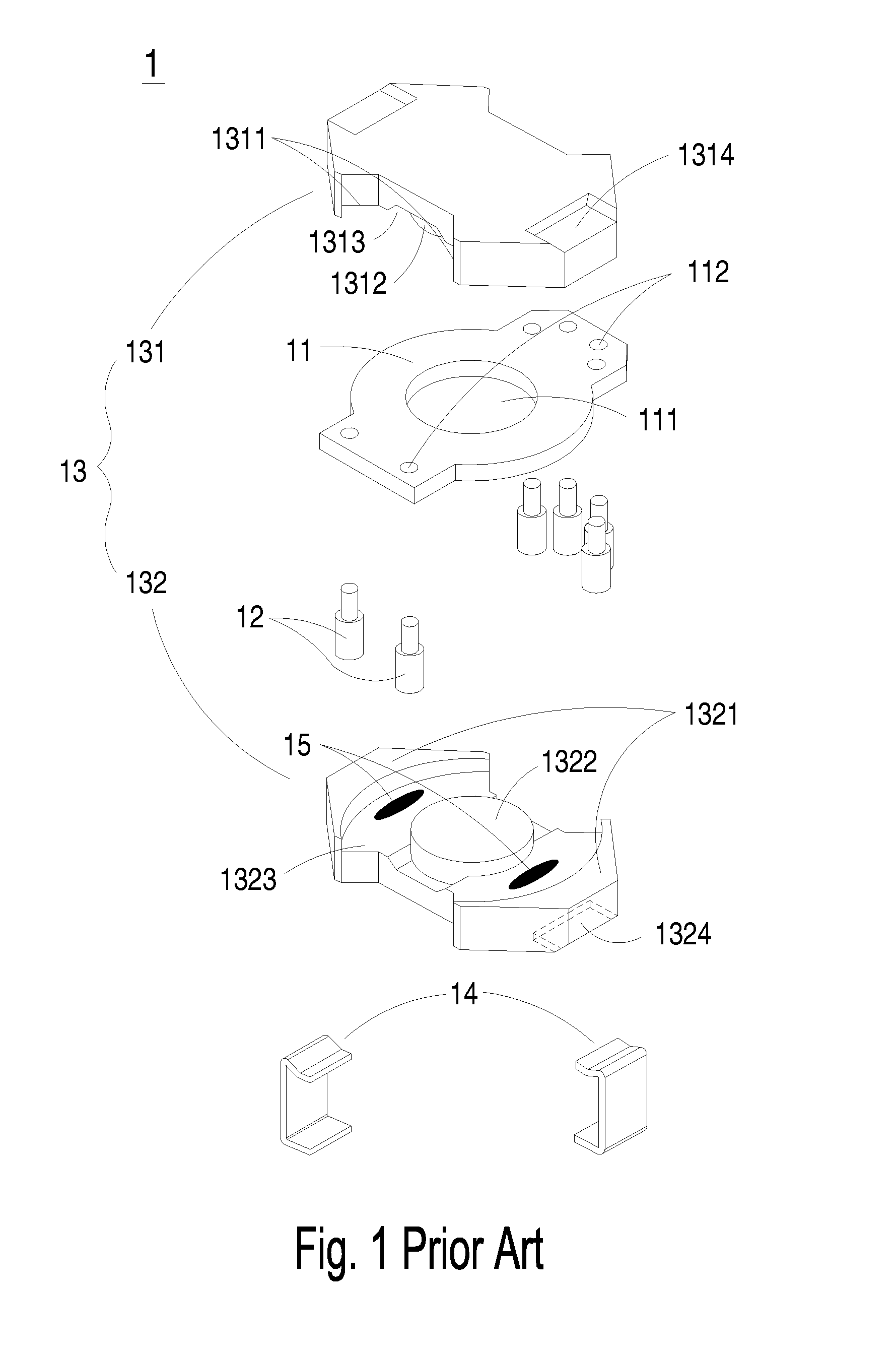
In addition, since the area of the second indentation 1323 of the second magnetic part 132 is small, it is difficult to manipulate the dispensing procedure.
The tilted circuit board 11 results in unevenness of the pins 12.
Therefore, the pins fail to be fixed onto the system circuit board due to the poor wetting property and the poor solderability.
Since the air contained in the gap is not a good thermally-conductive medium, the heat-dissipating efficiency of the transformer 1 is unsatisfied to meet the increasing power requirement of the power supply apparatus or power adapters.

Method used


Image

  • Transformer and assembling process thereof
  • Transformer and assembling process thereof
  • Transformer and assembling process thereof

Examples


Embodiment Construction

[0024]The present invention will now be described more specifically with reference to the following embodiments. It is to be noted that the following descriptions of preferred embodiments of this invention are presented herein for purpose of illustration and description only. It is not intended to be exhaustive or to be limited to the precise form disclosed.

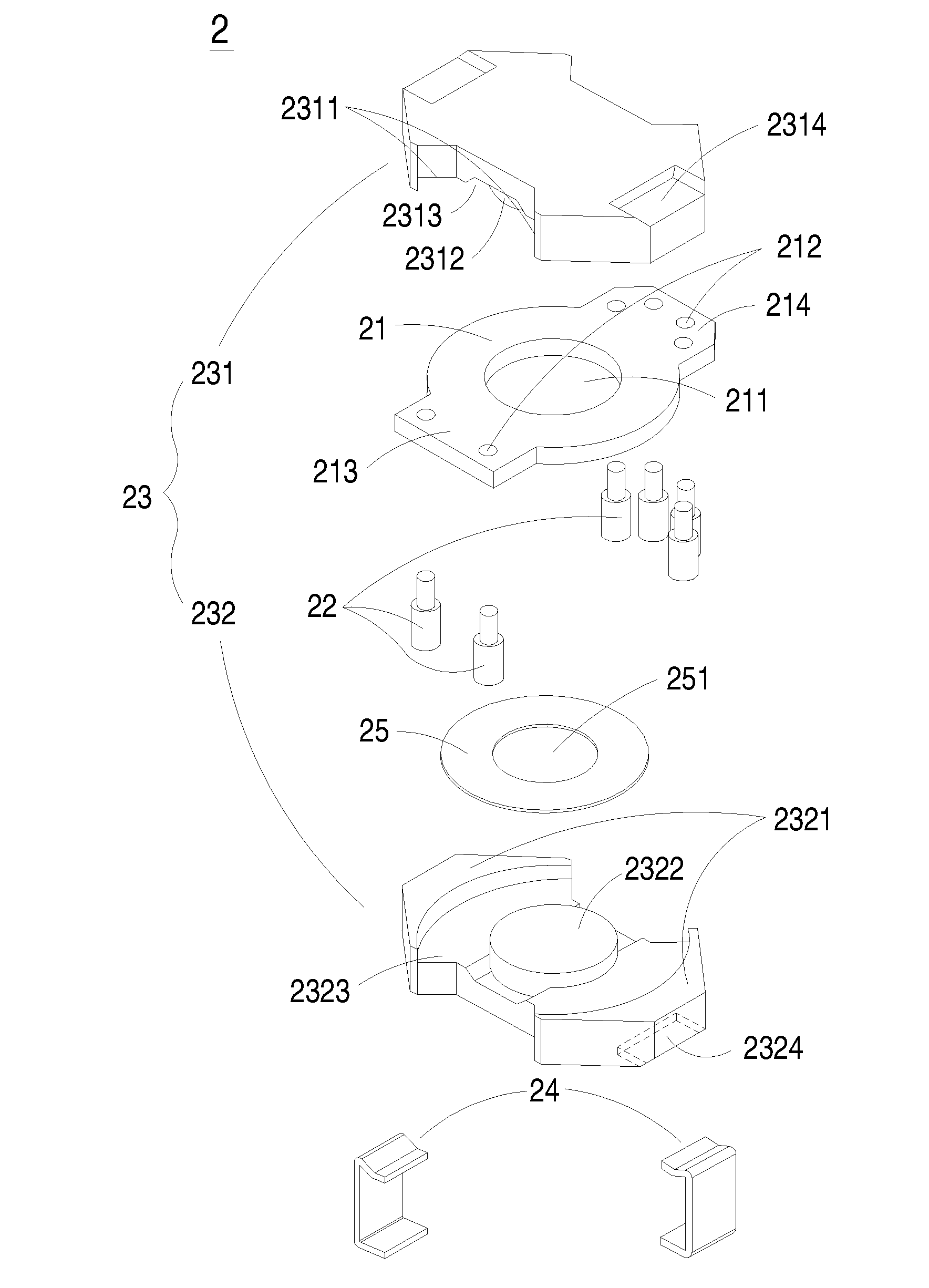
[0025]Referring to FIG. 3, a schematic exploded view of a transformer according to a preferred embodiment of the present invention is illustrated. The transformer 2 of FIG. 3 is a SMD (Surface Mount Device) transformer, which includes a circuit board 21, a plurality of pins 22, a magnetic core assembly 23 and at least an interface layer 25. The circuit board 21 is for example multi-layered circuit board and has thereon winding coil patterns including a primary winding coil and at least a secondary winding coil (not shown). The principle of designing the winding coil patterns is known in the art, and is not redundantly described h...


PUM

PropertyMeasurementUnit
conductiveaaaaaaaaaa
thicknessaaaaaaaaaa
sizeaaaaaaaaaa

Abstract

A transformer includes a magnetic core assembly, a circuit board, a plurality of pins and at least an interface layer. The magnetic core assembly includes a first magnetic part and a second magnetic part. The circuit board is arranged between the first magnetic part and the second magnetic part, and has a winding coil patterns including a primary winding coil and at least a secondary winding coil. The pins have first ends mounted onto the circuit board. The interface layer is arranged between the first magnetic part and the circuit board and / or between the second magnetic part and the circuit board such that the circuit board lies flat on the interface layer and is secured to the first magnetic part or the second magnetic part via the interface layer.

Description

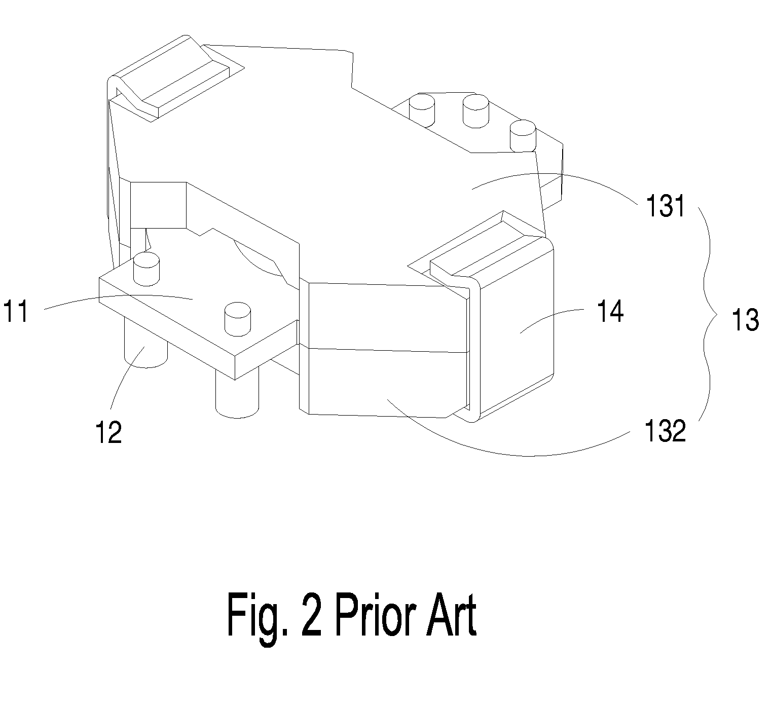
FIELD OF THE INVENTION[0001]The present invention relates to a transformer and a process of assembling the transformer.BACKGROUND OF THE INVENTION[0002]Transformers have become essential electronic components for various electronic devices such as power supply apparatus or power adapters. Since the electronic devices are developed toward small size and high power, the size of the transformers contained in the electronic devices should be minimized. Referring to FIG. 1, a schematic exploded view of a conventional transformer is illustrated. The transformer 1 of FIG. 1 principally comprises a circuit board 11, a plurality of pins 12, a magnetic core assembly 13 and a fixture member 14. The circuit board 11 is for example multi-layered circuit board and has thereon winding coil patterns including a primary winding coil and at least a secondary winding coil (not shown). The circuit board 11 has a hollow portion 111 at the center thereof and a plurality of conductive holes 112. The condu...

Claims


Application Information

Patent Timeline
Patent Type & Authority Patents(United States)
IPC IPC(8): H01F27/28H01F27/24
CPCH01F27/027H01F27/266H01F27/22H01F27/2804H01F27/292
Inventor CHENG, JUI-CHULIN, TSAI-SHENHSU, SU-CHIUNG
Owner DELTA ELECTRONICS INC
Learn More