Electronic image evaluating device and evalution method

a technology of electronic image and evaluating device, which is applied in the direction of instruments, material analysis, geological measurements, etc., can solve the problems of insufficient dependability and insufficient spatial interrelation between imaged objects, and achieve the effect of reducing the amount of image data to be processed and reducing resolution

Inactive Publication Date: 2008-05-20
KOENIG & BAUER AG
View PDF17 Cites 13 Cited by
  • Summary
  • Abstract
  • Description
  • Claims
  • Application Information

AI Technical Summary

Benefits of technology

[0012]Furthermore, the pixels of at least one area sensor, for example a CMOS or complementary metal oxide silicon sensor, can also be read out only partially. Individual image areas can thus be selectively blanked out in order to reduce the amount of image data to be processed. From these data, it is possible to determine the position of a segment, as well as to obtain image data of a segment with reduced resolution.
[0014]To be able to increase the scanning area which can maximally be observed by the image evaluating device, without having to employ correspondingly larger and larger area sensors, it is possible to provide several area sensors in the image evaluating device. The image data from the several individual area sensors are evaluated together in the downstream located evaluating device. As a result, it is possible to achieve, by the combination of several area sensors, the evaluation of a very large maximally observable scanning area with the image evaluating device by using relatively inexpensive standard components.
[0016]In order to be able to evaluate a printed product with great effectiveness, by utilization of the image evaluating device, a conveying arrangement should be provided in the image evaluating device, by the use of which conveying arrangement the printed product can be conveyed past the area sensor. In this connection, it is particularly advantageous if the pixels of the several individual area sensors can be selected and evaluated as a function of the conveying movement of the printed product. As a result, it can be achieved that the segments selected for observation by the several individual area sensors are selected as a function of the conveying movement of the printed product.

Problems solved by technology

In line camera systems, the spatial interrelation of the imaged objects is not assured with the required dependability because of the chronological synchronization of the image lines, which cannot always be maintained.

Method used


Image

  • Electronic image evaluating device and evalution method
  • Electronic image evaluating device and evalution method
  • Electronic image evaluating device and evalution method

Examples


Embodiment Construction

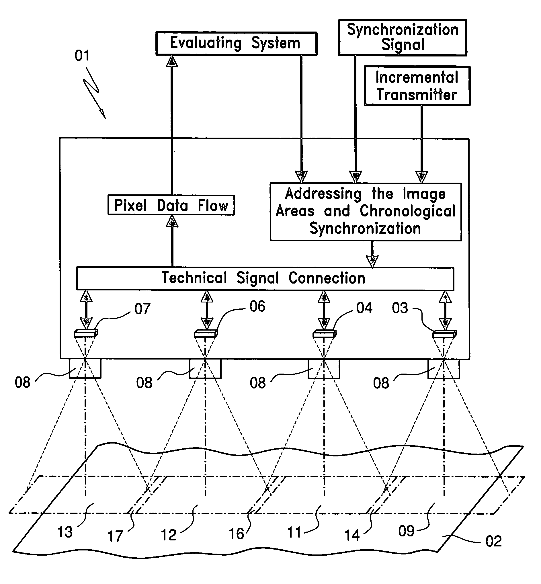
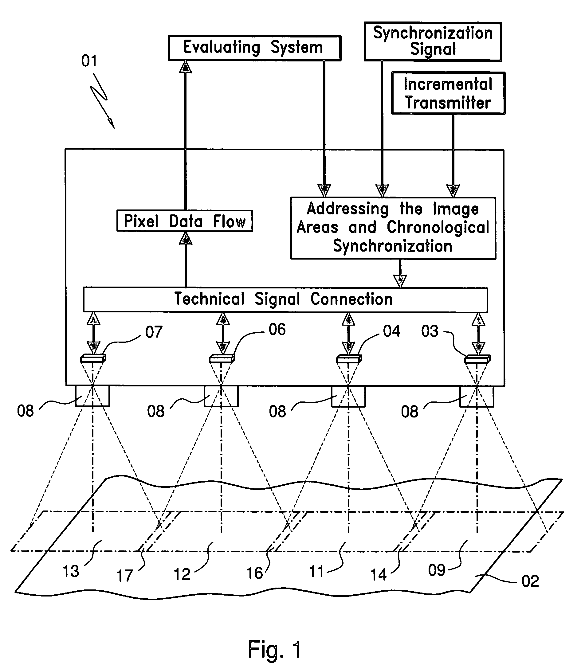
[0025]Referring initially to FIG. 1, there may be seen an image evaluating device, generally at 01, in accordance with the present invention. In the image evaluating device 01, which is schematically represented in FIG. 1, a web 02 of imprinted material can be conveyed underneath an area sensor system with four individual area sensors 03, 04, 06 and 07. These individual area sensors 03, 04, 06, and 07 are arranged on a common support element. An optical unit 08 is assigned to each of the individual area sensors 03 to 07, by the use of which optical units 08 a defined image area of the web 02 of imprinted material is produced on the light-sensitive pixels of the several individual area sensors 03 to 07.

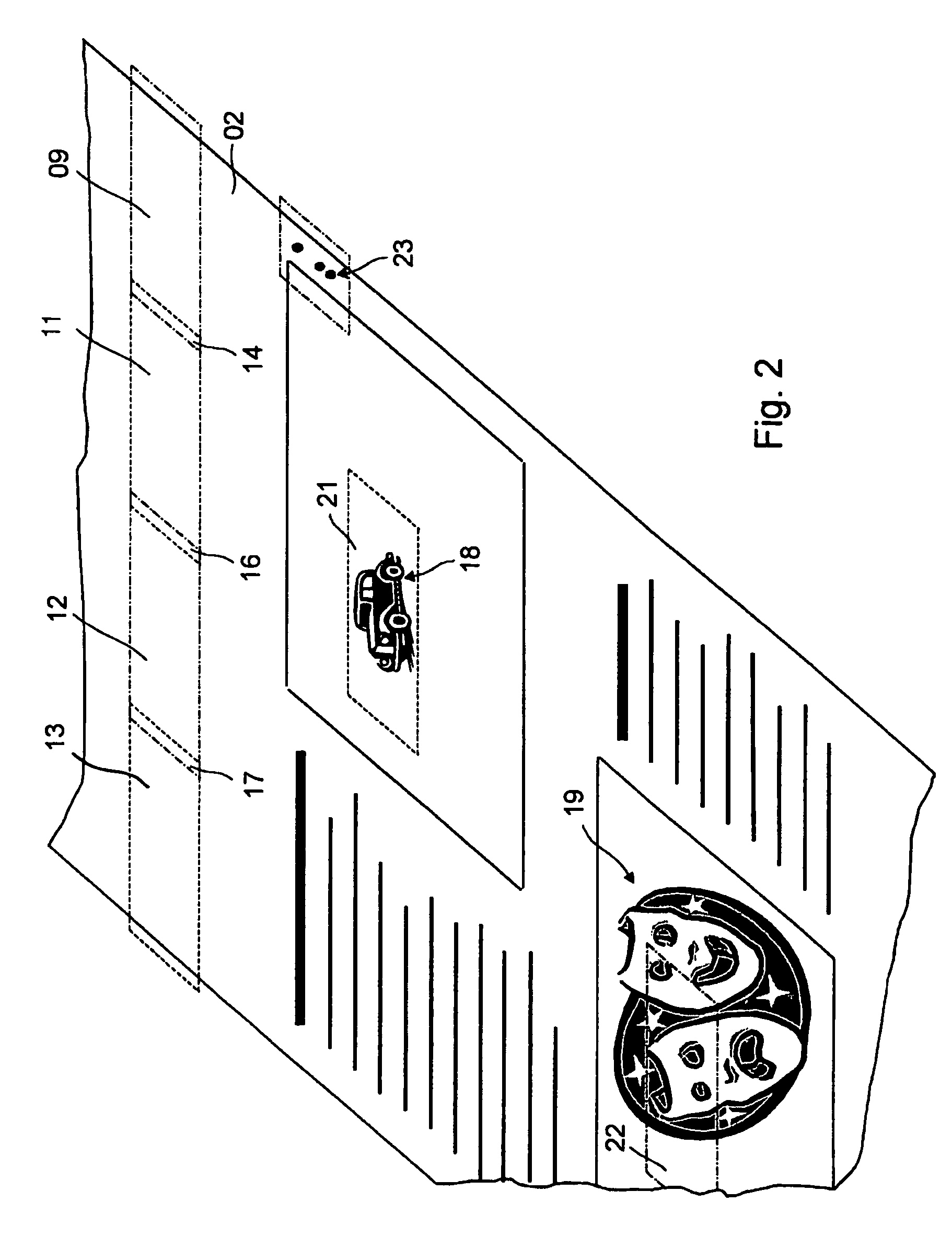
[0026]Maximally observable scanning areas 09, 11, 12 and 13 are a result of the type of area sensors 03 to 07 used, the properties of the optical units 08 used with the area sensors and the distance between the optical units 08 and the web 02 of imprinted material, which web 02 of impr...


PUM

PropertyMeasurementUnit
strengthaaaaaaaaaa
areaaaaaaaaaaa
areasaaaaaaaaaa

Abstract

An electronic image evaluating device includes at least one area sensor that is provided with a plurality of photosensitive pixels. Each of these pixels will emit an electric output signal in response to the light input signal that it receives. The intensity of the electric output signal correlates with the light input signal. This electric output signal is evaluated in an evaluation unit as image information. The pixels of the area sensor can be controlled and evaluated individually, or in groups. Any sector of the maximum monitorable scanning area can be selectively evaluated.

Description

CROSS-REFERENCE TO RELATED APPLICATIONS[0001]This patent application is the U.S. National Phase under 35 USC 371 of PCT / DE 03 / 00569, filed Feb. 22, 2003; published as WO 03 / 073084 A1 on Sep. 4, 2003 and claiming priority to DE 102 08 286.3, filed Feb. 26, 2002, the disclosures of which are expressly incorporated herein by reference.FIELD OF THE INVENTION[0002]The present invention is directed to a method for using an electronic image evaluating device. The device has at least one area sensor with a plurality of light-sensitive pixels. The pixels can be triggerable and evaluated individually or in groups.BACKGROUND OF THE INVENTION[0003]Electronic image evaluating devices for checking printed products are known, with which evaluating devices defined features of a printed product can be recorded and evaluated. Normally, individually adapted sensors or cameras are used for checking these special features. Since the position of these features, or the number of features to be evaluated c...

Claims


Application Information

Patent Timeline
Patent Type & Authority Patents(United States)
IPC IPC(8): G06K9/00G01N21/89
CPCG01N21/8903
Inventor STOBER, BERND RUDIGER
Owner KOENIG & BAUER AG
Why Eureka
Try Eureka