Tabbed circuit board and method for manufacturing same

a technology of tabbed circuit boards and tabs, which is applied in the direction of display means, semiconductor devices for light sources, lighting and heating apparatus, etc., can solve the problems of weakened legs, weakened leds, and prone to breaking, and achieve compact profile and prevent any weakening of legs

Inactive Publication Date: 2008-05-27
ILIGHT TECH INC
View PDF4 Cites 31 Cited by
  • Summary
  • Abstract
  • Description
  • Claims
  • Application Information

AI Technical Summary

Benefits of technology

[0006]The integral tabs can then be manipulated from the first position to a second position, in which each tab is oriented at an angle (for example, substantially perpendicular) relative to the remainder of the substrate. By manipulating the tabs from the first position to the second position in this manner, there is neither bending nor other manipulation of the legs of the LEDs. Accordingly, no stresses are applied to the legs o

Problems solved by technology

However, the legs are weakened and may become susceptible to breaking when so manipulated.
Furthermore, and perhaps more importantl

Method used


Image

  • Tabbed circuit board and method for manufacturing same
  • Tabbed circuit board and method for manufacturing same
  • Tabbed circuit board and method for manufacturing same

Examples


Embodiment Construction

[0015]The present invention is a tabbed circuit board populated with electrical components and method for manufacturing same.

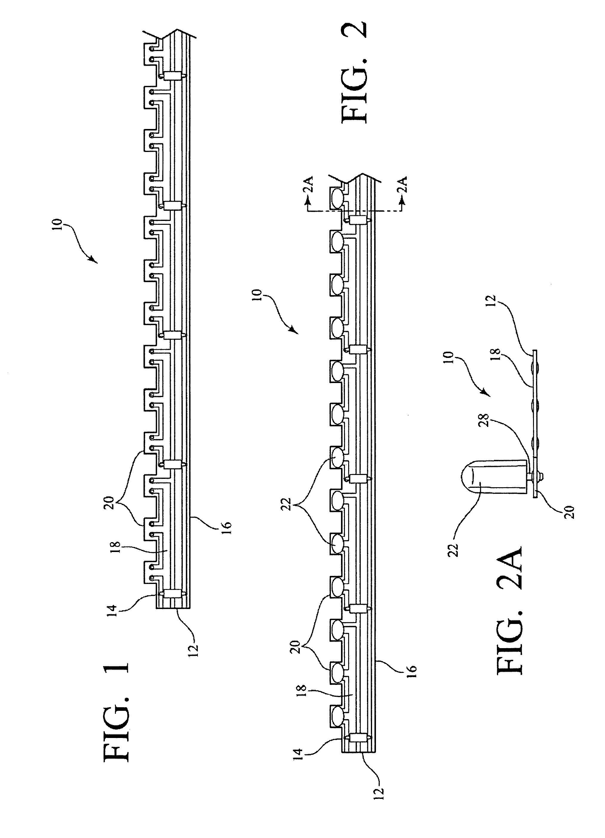
[0016]FIG. 1 is a partial plan view of an exemplary tabbed circuit board 10 made in accordance with the present invention. The tabbed circuit board 10 includes a flexible substrate 12 of a predetermined length, having a first lateral edge 14 and a second lateral edge 16. The flexible substrate 12 further has a plurality of integral tabs 20 arrayed along the first lateral edge 14, the importance of which is further described below. A conductive trace 18 is applied to the flexible substrate 12. The conductive trace 18 would commonly be applied by adhering a layer of copper over the substrate 12, and then removing unwanted copper through chemical etching or a similar technique; however, other manufacturing methods could certainly be used to apply the conductive trace 18 without departing from the spirit and scope of the present invention.

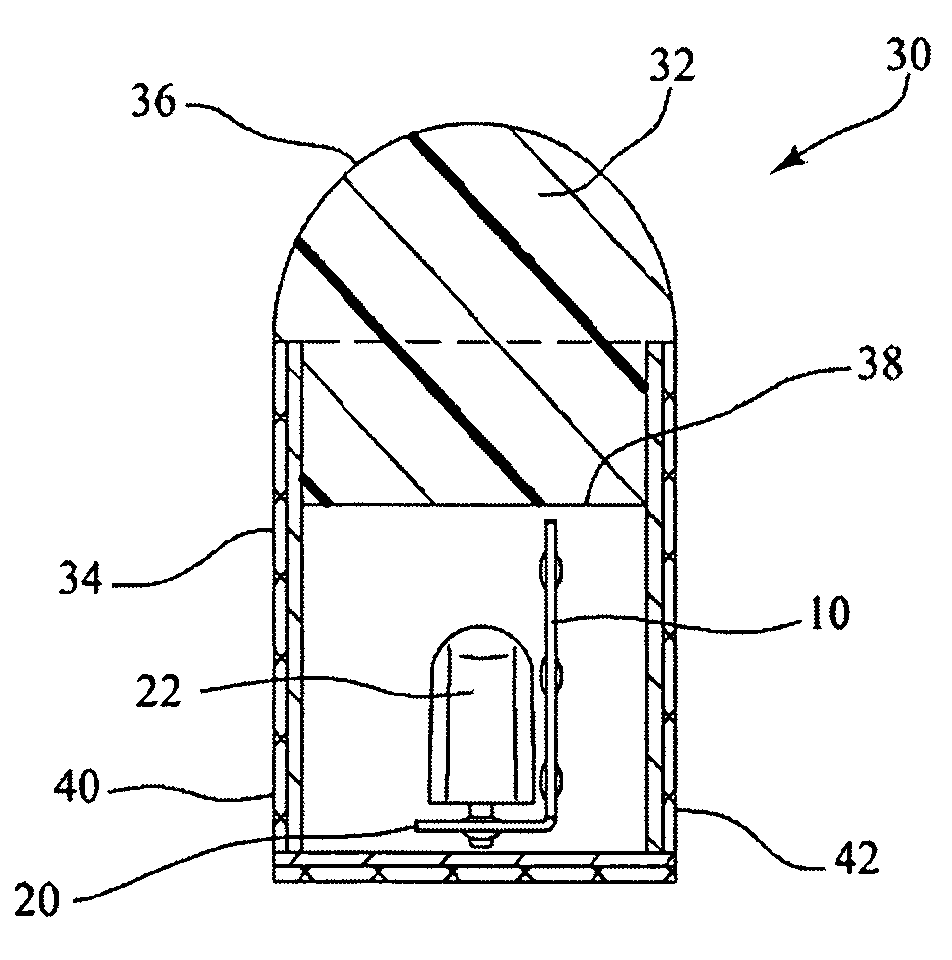
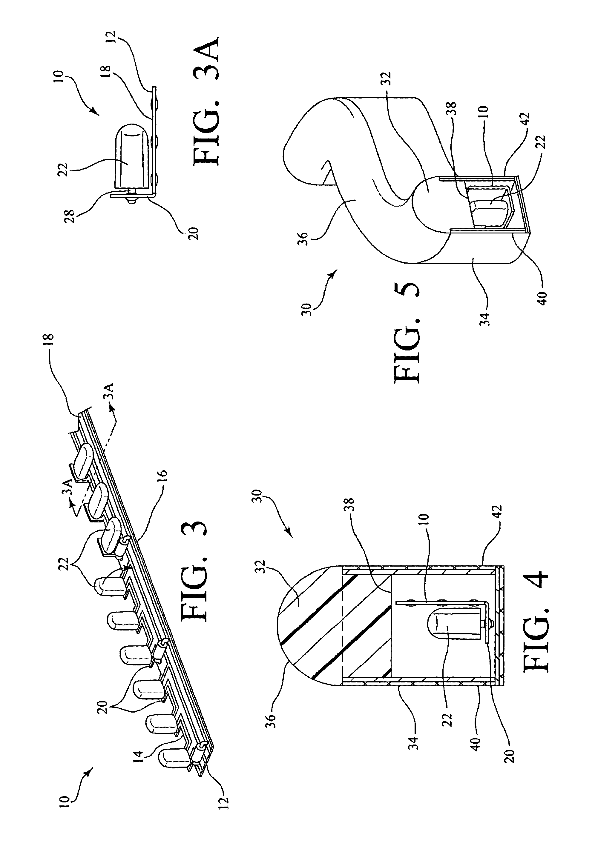
[0017]Referring now to FI...


PUM


Abstract

A circuit board for receiving and operably connecting a plurality of electrical components generally comprises: a flexible substrate of a predetermined length and having a first lateral edge and a second lateral edge; a conductive trace applied to the flexible substrate; and a plurality of integral tabs arrayed along the first lateral edge, one or more electrical components being operably connected to the conductive trace at a respective tab, and wherein each tab can be manipulated from a first position in which the tab is aligned with the remainder of the substrate to a second position in which the tab is oriented at an angle relative to the remainder of the substrate.

Description

BACKGROUND OF THE INVENTION[0001]The present invention is a tabbed circuit board populated with electrical components and method for manufacturing same.[0002]Light-emitting diodes (LEDs) are useful in various lighting applications. Since the development of LEDs, many attempts have been made to utilize them in innovative ways. For example, U.S. Pat. Nos. 6,592,238 and 6,953,262, which are incorporated herein by this reference, each describe the use of LEDs in an illumination device to simulate neon lighting. The use of LEDs offer many advantages compared with neon lighting including, for example, better durability and reduced costs. As described in U.S. Pat. Nos. 6,592,238 and 6,953,262, a circuit board is typically populated with LEDs and placed in a housing adjacent the light-receiving surface of a rod-like member or waveguide. The rod-like member / waveguide is made of a material that preferentially scatters light entering the light-receiving surface such that the light intensity pa...

Claims


Application Information

Patent Timeline
IPC IPC(8): H01R12/00
CPCF21S4/003H05K1/189F21Y2101/02H05K2201/046H05K2201/091H05K2201/09172H05K2201/10106H05K2201/10446F21S4/20F21Y2115/10Y10S362/80
Inventor ERIKSSON, ERIC O.
Owner ILIGHT TECH INC
Why Eureka
Try Eureka