Modular I/O bank architecture

a module and i/o bank technology, applied in the field ofprogrammable devices, can solve the problems of limiting the designers' flexibility in circuit board layout, increasing the cost of implementing a design, and most i/o banks can only be configured to support a single interface, so as to facilitate circuit board layout

Inactive Publication Date: 2008-05-27
ALTERA CORP
View PDF14 Cites 24 Cited by
  • Summary
  • Abstract
  • Description
  • Claims
  • Application Information

AI Technical Summary

Benefits of technology

[0012]In an embodiment, a programmable device I / O architecture allows for a variable number of I / O banks. Each I / O bank is of an I / O bank type. Each I / O bank type has a fixed number of I / O pins. I / O banks of the same I / O bank type are compatible within the same programmable device and between different types of programmable devices. The number of I / O pins for each I / O bank type is selected so that each of a set of interfaces can be implemented efficiently using I / O banks of at least one I / O bank type. In a further embodiment, the largest size I / O bank type and intermediate size I / O bank types are adapted to be a compatible supersets of every smaller I / O bank type. In another embodiment, the ratio between data pins and support pins in each I / O bank type is the same. In a further embodiment, support pins are regularly distributed between data pins in each I / O bank type. In a further embodiment, multiple instances of the same or compatible I / O bank types are arranged to be accessible from different sides of the programmable device. To facilitate circuit board layout, an embodiment of the programmable device architecture arranges the pins of each I / O bank as a mirror and / or rotation of pins of other I / O banks on the device.

Problems solved by technology

The use of a fixed number of I / O banks and a variable number of I / O pins per I / O bank in a programmable device architecture presents a number of problems.
First, most I / O banks can only be configured to support a one interface at a time.
This often forces designers to use programmable devices with even more I / O pins to ensure that there are sufficient I / O pins available to support the required interfaces, which further increases the costs of implementing a design.
Additionally, these restrictions on I / O pin usage limit the designers' flexibility in circuit board layout.
Vertical migration is another problem arising from prior programmable device architectures that use of a fixed number of I / O banks and a variable number of I / O pins per bank.
However, prior programmable device architectures having a fixed number of I / O banks and a variable number of I / O pins per bank often require substantial reengineering for vertical migration.
For example, because the number of I / O pins per I / O bank often increases for a larger devices, the I / O banks of the larger device may not support the same I / O pin assignments as the corresponding I / O banks in the smaller device.
Noise, clock skew, and signal reflection are other problems arising in vertical migration that are caused by the use of a fixed number of I / O banks and a variable number of I / O pins per bank.
As the number of pins per I / O bank increase, the total number of active switches and other components associated with I / O pins increases, thereby increasing the amount of noise and signal reflections introduced.

Method used


Image

  • Modular I/O bank architecture
  • Modular I/O bank architecture
  • Modular I/O bank architecture

Examples


Embodiment Construction

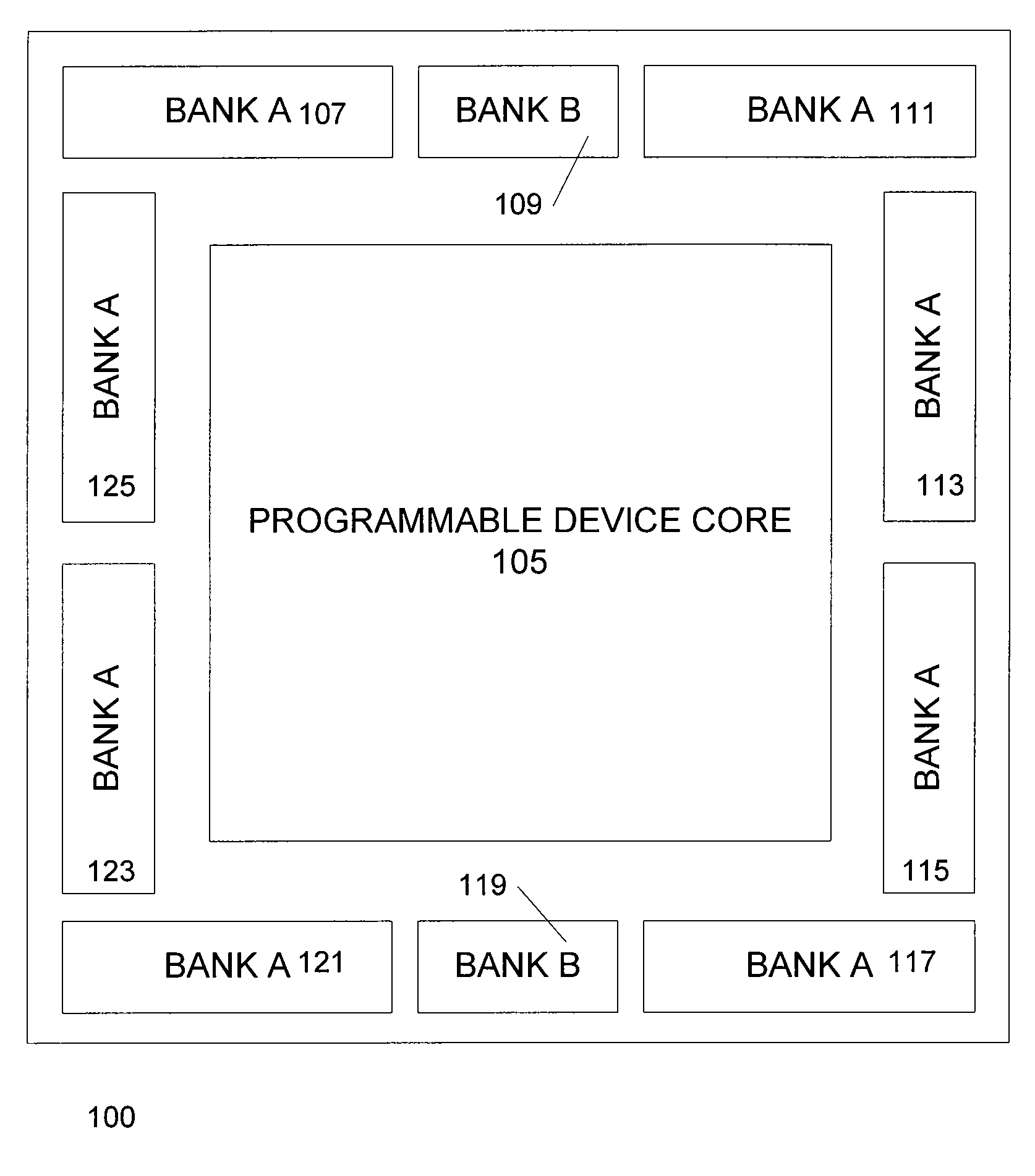
[0022]FIG. 1 illustrates a programmable device and I / O bank architecture 100 according to an embodiment of the invention. Device architecture 100 includes a programmable device core 105. Programmable device core 105 includes programmable device components such as logic cells, functional blocks, memory units, and a configurable switching circuit.

[0023]Device architecture 100 includes a plurality of I / O banks, such as I / O banks 107, 109, 111, 113, 115, 117, 119, 121, 123, and 125. In an embodiment, device architecture 100 allows for any number of I / O banks.

[0024]In an embodiment, the plurality of I / O banks belong to a limited number of I / O bank types. For example, I / O banks 107, 111, 113, 115, 117, 121, 123, and 125 are of I / O bank type A. I / O banks 109 and 119 belong to I / O bank type B. Each I / O bank type specifies the number of I / O pins and other attributes for its member I / O banks. For example, type A I / O banks may have 60 I / O pins and type B I / O banks may have 36 I / O pins. The num...


PUM


Abstract

A programmable device I / O architecture allows for a variable number of I / O banks. Each I / O bank is of an I / O bank type. Each I / O bank type has a fixed number of I / O pins. I / O banks of the same I / O bank type are compatible within the same programmable device and between different types of programmable devices. The largest size I / O bank type and intermediate size I / O bank types are adapted to be a compatible supersets of every smaller I / O bank type. Support pins are regularly distributed between data pins in each I / O bank type. Multiple instances of the same or compatible I / O banks are arranged to be accessible from different sides of the programmable device. To facilitate circuit board layout, each I / O bank is arranged as a mirror and / or rotation of other I / O banks on the device.

Description

CROSS-REFERENCE TO RELATED APPLICATIONS[0001]This application is a continuation-in-part to U.S. patent application Ser. No. 11 / 337,046, filed Jan. 19, 2006, and entitled “Modular I / O Bank Architecture,” which is incorporated by reference herein for all purposes.BACKGROUND OF THE INVENTION[0002]The present invention relates to the field of programmable devices, and the systems and methods for programming the same. Programmable devices, such as FPGAs, typically includes thousands of programmable logic cells that use combinations of logic gates and / or look-up tables to perform a logic operation. Programmable devices also include a number of functional blocks having specialized logic devices adapted to specific logic operations, such as adders, multiply and accumulate circuits, phase-locked loops, and one or more embedded memory array blocks. The logic cells and functional blocks are interconnected with a configurable switching circuit. The configurable switching circuit selectively rou...

Claims


Application Information

Patent Timeline
Patent Type & Authority Patents(United States)
IPC IPC(8): H03K19/173
CPCH03K19/17744
Inventor TYHACH, JEFFREYSUNG, CHIAKANGNGUYEN, KHAICHARAGULLA, SANJAY K.BURNEY, ALI
Owner ALTERA CORP
Why Eureka
Try Eureka