Semiconductor memory device
a memory device and semiconductor technology, applied in the direction of information storage, static storage, digital storage, etc., can solve the problems of inability to speed up the cycle, inability to shorten the write operation cycle further, and the parasitic load element in the connecting node is extremely small, so as to improve the chip performance and improve the chip performance
- Summary
- Abstract
- Description
- Claims
- Application Information
AI Technical Summary
Benefits of technology
Problems solved by technology
Method used
Image


Examples
Embodiment Construction
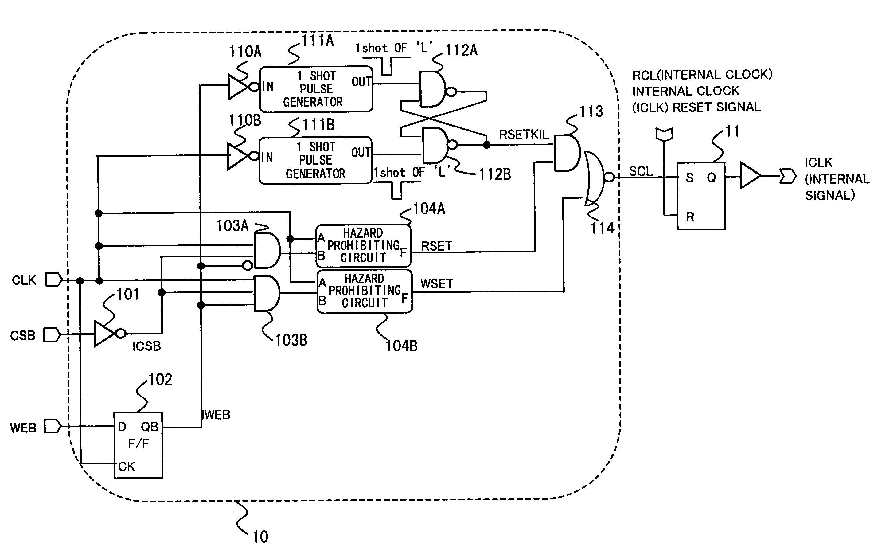
[0060]Referring to the drawings, certain preferred embodiments of the present invention will be described in detail. FIG. 1 is a diagram illustrating the configuration of essential portions of a semiconductor memory device according to an embodiment of the present invention. In the present embodiment, the method for controlling the read operation of the RAM itself is the same as a conventional control method described with reference to e.g. FIG. 11A. The present embodiment is provided with a circuit for canceling internal clock generation 10 (see FIG. 1) within the RAM for canceling the internal operation of the RAM of a cycle next following the write operation, and the manner for controlling write operation according to the present embodiment differs from the conventional controlling manner.
[0061]More specifically, the circuit for canceling internal clock generation 10 of the present embodiment, shown in FIG. 1, includes, only by way of illustration, a CLK terminal, as a terminal f...
PUM
 Abstract
Description
Claims
Application Information