
Shallow trench isolation area having buried capacitor

a capacitor and trench isolation technology, applied in the field of semiconductor devices, can solve the problems of inefficiency, achieve the effect of improving chip performance, high capacitance level, and efficient utilization of chip spa

Inactive Publication Date: 2014-11-25
INFINEON TECH AG
View PDF12 Cites 7 Cited by
  • Summary
  • Abstract
  • Description
  • Claims
  • Application Information

AI Technical Summary

Benefits of technology

[0012]Aspects of the present invention solve these problems in the related art by concealing buffer capacitors in the existing, but otherwise unused, STI (Shallow Trench Isolation) area of the semiconductor chip, which is generally distributed throughout the entire chip. As a result, the chip space is more efficiently utilized, thereby improving chip performance. Furthermore, since the STI areas are distributed throughout the semiconductor chip, the buffer capacitors can likewise be distributed throughout the chip, achieving a sufficiently high level of capacitance to protect the electrical components. Moreover, the buffer capacitance can be distributed equally across the entire chip. The result is a smaller chip area and greater effectiveness in use of the corresponding capacitance. The smaller chip area also results in lower costs per chip.

Problems solved by technology

Furthermore, the area-neutral parasitic capacitors contribute only a relatively small amount to the overall capacitance that is required, and are also rather inefficient due to the high-resistance lines frequently employed in their design.

Method used


Image

  • Shallow trench isolation area having buried capacitor
  • Shallow trench isolation area having buried capacitor
  • Shallow trench isolation area having buried capacitor

Examples


first embodiment

[0046]FIG. 3 depicts a cross-sectional view of a semiconductor chip having STI areas with buried buffer capacitors according to a As shown in FIG. 3, a semiconductor chip 10 includes a shallow trench isolation (STI) area 11 having buffer capacitors 12 buried therein, where the buffer capacitors 12 are arranged in a buried line-to-line configuration in which the buffer capacitors 12 are connected via lines in a serial fashion. In this embodiment, the STI area 11 separates the active transistor region 17 and the substrate contact region 18 from each other to prevent electrical current leakage from affecting performance.

[0047]The semiconductor chip 10 further includes a metal layer 19 (M1) to transmit electric current. Additionally, the semiconductor chip 10 includes gate electrode stacks (GC) 19a. The gate electrode stacks 19a may be designed by adding a thin layer of gate oxide on top of the silicon surface 14, adding a conducting layer of polysilicon over the gate oxide, and then a...

third embodiment

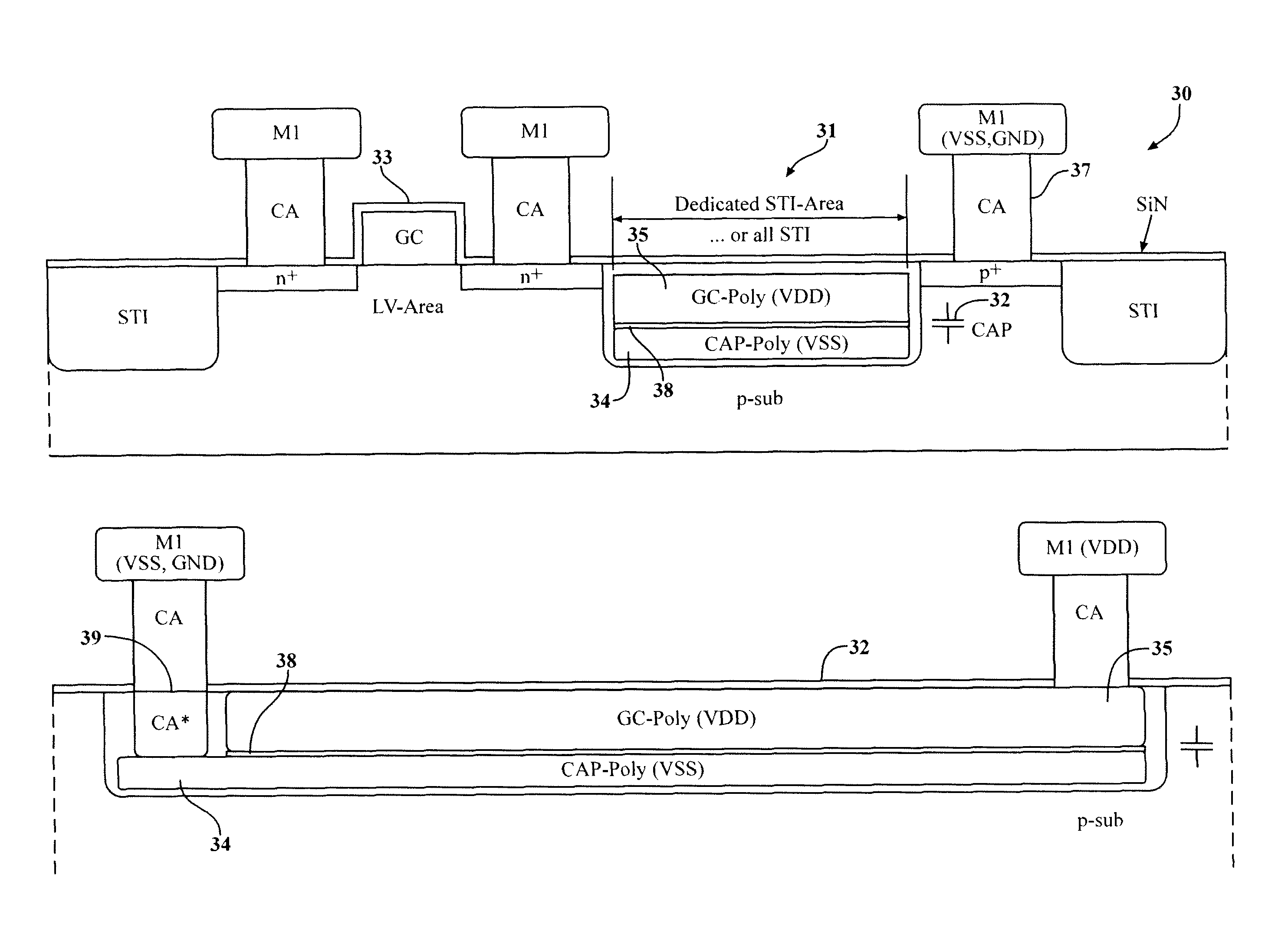
[0056]FIG. 5a depicts a cross-sectional view of a semiconductor chip having STI areas with buried buffer capacitors according to a As shown in FIG. 5a, a semiconductor chip 30 includes a shallow trench isolation (STI) area 31 having a buffer capacitor 32 completely buried therein (STI B CAP). The buffer capacitor 32 has a lower plate 34 and an upper plate 35 separated by an insulator 38. The STI area 31 separates the active transistor region 33 and the substrate contact region 37 from each other to prevent electrical current leakage from affecting performance.

[0057]As shown in the bottom of FIG. 5a, which depicts an exploded view of the third STI area 31, this third embodiment also uses a classic parallel plate capacitor design of two electrically conducting plates 34 and 35 that are separated from each other by an insulator 38 and arranged horizontally above each other. The plates 34 and 35 are distinguished from conventional architecture since they are completely buried in the ST...

fourth embodiment

[0059]FIG. 6 depicts a cross-sectional view of a semiconductor chip having STI areas with buried buffer capacitors according to a As shown in FIG. 6, a semiconductor chip 40 includes a shallow trench isolation (STI) area 41 having multiple buffer capacitors 42 buried therein. Each of the buffer capacitors 42 includes a lower plate 44 and an upper plate 45 separated by an insulator 48. The STI area 41 separates the active transistor region 43 and the substrate contact region 47 from each other to prevent electrical current leakage from affecting performance.

[0060]As shown in the bottom of FIG. 6, which depicts an exploded view of the STI area 41, this fourth embodiment is similar to the third embodiment, but employs multiple buried layers of buffer capacitors 42. The STI area 41 includes n numbers of buffer capacitors 42, where n is two or more. The plates of the buffer capacitors 42 are disposed to be substantially parallel to a surface 46 of the semiconductor chip 40. As a result,...


PUM


Abstract

A semiconductor chip includes a substrate including a surface, an active transistor region and a substrate contact region formed on the substrate, a shallow trench isolation (STI) area formed in the surface and disposed at least partially between the active transistor region and the substrate contact region, and at least one capacitor at least partially buried in the STI area.

Description

CROSS-REFERENCE TO RELATED APPLICATIONS[0001]1. Field of the Invention[0002]The present invention relates to semiconductors, and more particularly, relates to an apparatus and method to bury buffer capacitors in shallow trench isolation (STI) areas of semiconductor chips.[0003]2. Background of the Invention[0004]Integrated circuits (ICs) are miniaturized electronic circuits that typically include semiconductor devices as well as other components, and have widespread applications throughout the world of electronics. The semiconductor devices used within ICs include a number of electrical components disposed next to each other. Semiconductor devices are typically fabricated by sequentially depositing insulating or dielectric layers, conductive layers, and semiconductive layers of material over a semiconductor substrate, and patterning the various layers using lithography to form circuit components and elements thereon, forming integrated circuits.[0005]To prevent electrical current le...

Claims


Application Information

Patent Timeline
Patent Type & Authority Patents(United States)
IPC IPC(8): H01L29/00H01L27/06H01L49/02H01L29/94H01L27/02H01L29/66
CPCH01L29/945H01L27/0629H01L29/66181H01L28/65H01L27/0207H01L29/0653H01L21/823481H01L28/40H01L21/76224
Inventor TERLETZKI, HARTMUD
Owner INFINEON TECH AG
Learn More