Polycarbosilane buried etch stops in interconnect structures

a technology of polycarbosilane and interconnect structure, which is applied in the direction of electrical apparatus, semiconductor/solid-state device details, semiconductor devices, etc., can solve the problems of poor etch selectivity with other dielectric layers, system may not exhibit sufficient etch selectivity to silicon carbonitrides, silicon carbides, etc., to improve adhesion and coating quality.

Inactive Publication Date: 2007-03-06
TAIWAN SEMICON MFG CO LTD
View PDF8 Cites 7 Cited by
  • Summary
  • Abstract
  • Description
  • Claims
  • Application Information

AI Technical Summary

Benefits of technology

[0009]One aspect of the inventive buried etch stop layer is the unique chemical compositions that provide sufficient chemical contrast for dry etch processes used to define structural features in an interconnect structure. The processing of the inventive buried etch stop layer is facile as films can be applied by any solvent based process, e.g., spin coating. Additionally, the low dielectric constant (e.g. k≦3.3) of the buried etch stop layer contributes to reductions in resistance-capacitance delays, crosstalk, and power dissipation leading to enhanced chip performance. The present invention also provides many additional advantages, which shall become apparent as described below.
[0023]The polymeric material comprising the buried etch stop layer is soluble in an organic solvent and can be applied as a coating to form a buried etch stop layer by a solvent based process. The polymeric material comprising the buried etch stop layer can also be a mixture of two or more polymeric components; the polymeric materials having any chain architecture. The polymeric material comprising the buried etch stop layer may be comprised of at least one of the following: polysilazanes, polysilanes, polycarbosilanes, polysilasilazane, polysilylenemethylenes, polysilacarbosilanes, polysilylcarbodiimides, polysiloxazanes, polycarbosilazanes, polysilylenemethylenes, polysilsesquiazanes, and polysilacarbosilazanes. In addition, additives such as adhesion promoters and antistriation agents can be added to the solution containing the polymeric material to improve adhesion and coating quality, respectively.

Problems solved by technology

The application of spin-on dielectrics as buried etch stops has been proposed; however, current implementations have been primarily limited to silsequioxanes, siloxanes, and other related chemistries that are primarily based on silicon-oxygen bonds.
One potential drawback of these current implementations is poor etch selectivity with other dielectric layers.
In particular, these systems may not exhibit sufficient etch selectivity to silicon carbonitrides, silicon carbides, and silicon nitrides that are commonly used as cap barrier layers.
The lack of etch selectivity with these layers precludes the generation of integrated circuits in a controllable manner.

Method used


Image

  • Polycarbosilane buried etch stops in interconnect structures
  • Polycarbosilane buried etch stops in interconnect structures
  • Polycarbosilane buried etch stops in interconnect structures

Examples


Embodiment Construction

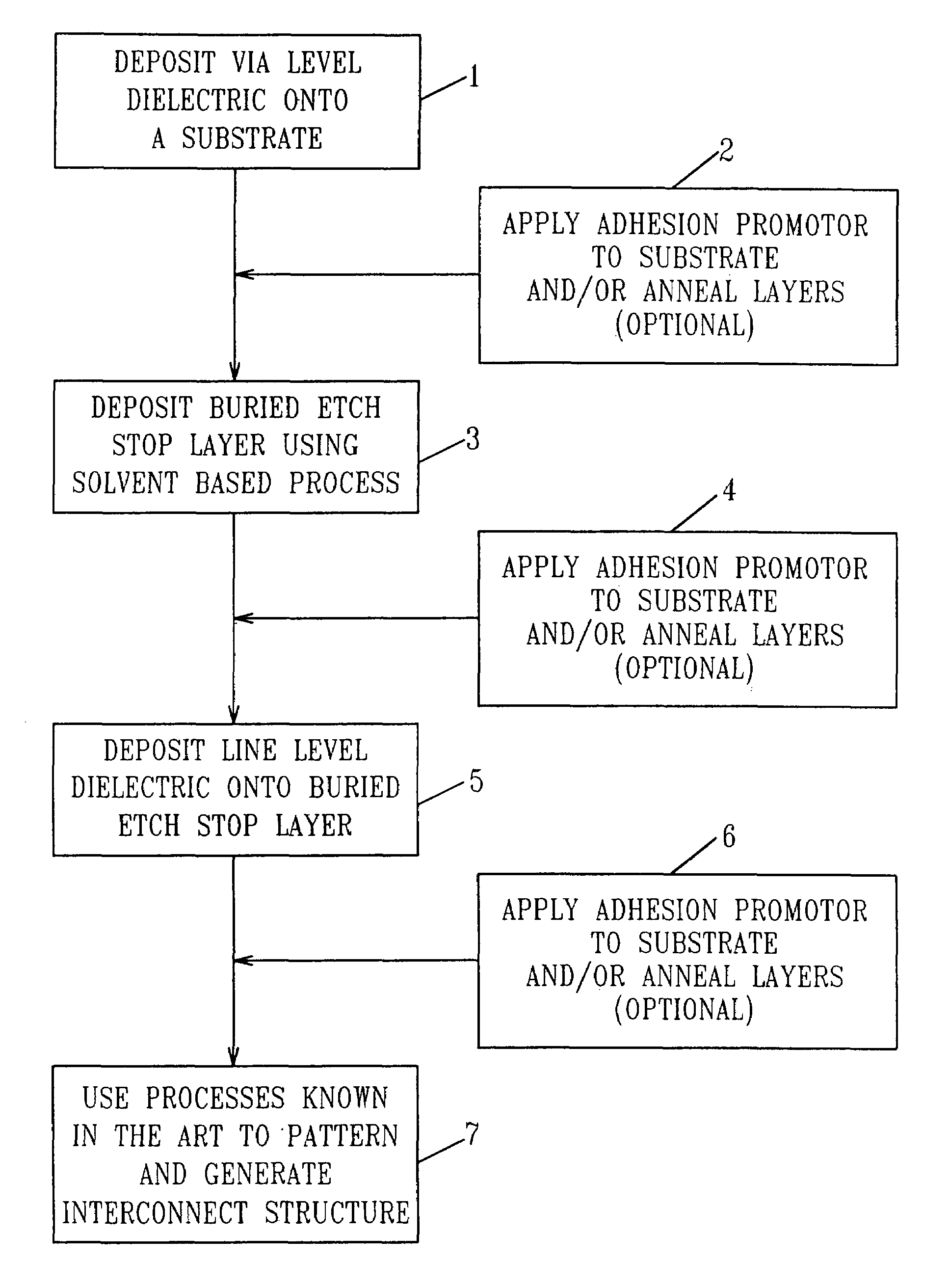
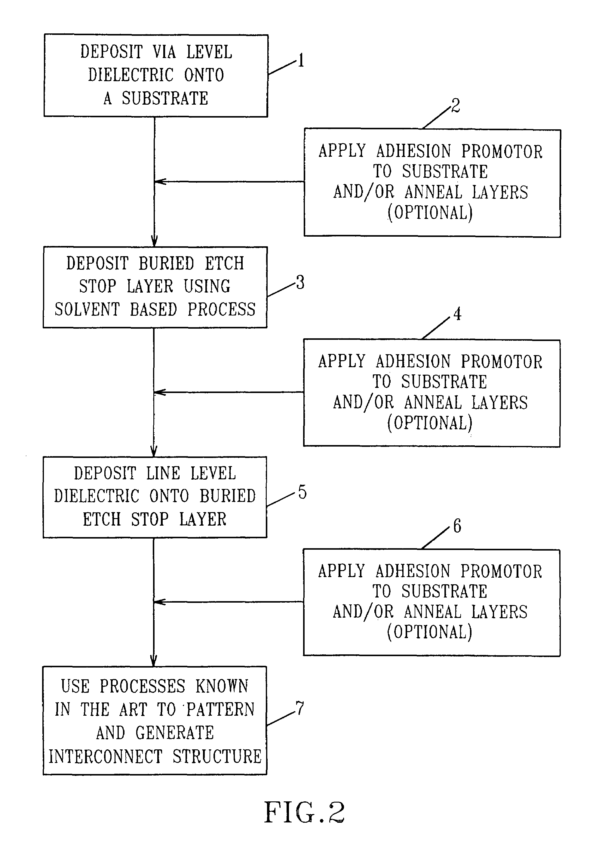
[0029]A detailed description of the structures and methods involving buried etch stop layers is presented below. The buried etch stop layers can be utilized to enable the fabrication of interconnects that can be used in any microelectronic device. It is noted that in the accompanying drawings like and corresponding elements are referred to by like reference numbers.

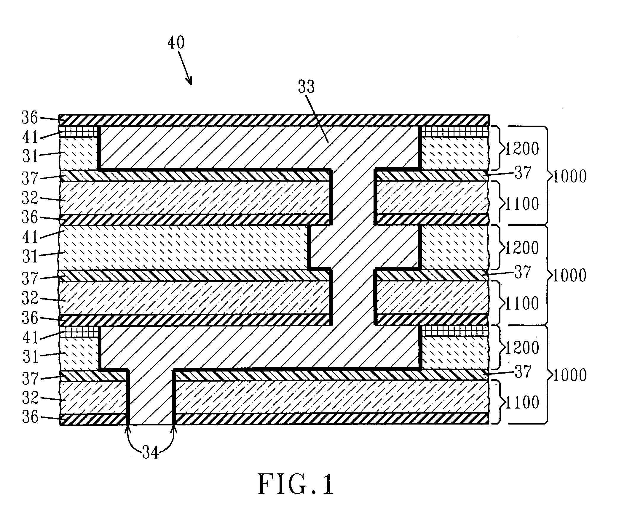
[0030]Referring to FIG. 1, in the first embodiment, an interconnect structure 40, is comprised of multiple levels 1000 where each level comprises of at least a via level interlayer dielectric 1100 and a line level interlayer dielectric 1200. The interconnect structure 40 comprises conducting metal features 33 that traverse through the structure and may have interfaces with a lining metal barrier 34. The conducting metal features 33 and lining metal barrier 34 are surrounded by dielectrics. The dielectrics in the via level interlayer dielectric 1100 include the via dielectric 32 and an optional cap barrier layer film 36, w...


PUM


Abstract

Interconnect structures having buried etch stop layers with low dielectric constants and methods relating to the generation of such buried etch stop layers are described herein. The inventive interconnect structure comprises a buried etch stop layer comprised of a polymeric material having a composition SivNwCxOyHz, where 0.05≦v≦0.8, 0≦w≦0.9, 0.05≦x≦0.8, 0≦y≦0.3, 0.05≦z≦0.8 for v+w+x+y+z=1; a via level interlayer dielectric that is directly below said buried etch stop layer; a line level interlayer dielectric that is directly above said buried etch stop layer; and conducting metal features that traverse through said via level dielectric, said line level dielectric, and said buried etch stop layer.

Description

CROSS REFERENCE TO RELATED APPLICATIONS[0001]The present invention claims benefit of U.S. provisional patent application 60 / 484,397 filed Jul. 2, 2003, the whole content and disclosure of which is incorporated by reference as is fully set forth herein. Additionally, the following U.S. Applications are incorporated herein by reference: Application Ser. No. 60 / 443,504 filed on Jan. 29, 2003, Application Ser. No. 60 / 443,361 filed on Jan. 29, 2003 and Application Ser. No. 60 / 463,758 filed on Apr. 17, 2003.FIELD OF THE INVENTION[0002]The present invention relates to the utilization of low dielectric constant buried etch stop layers in interconnect structures that are part of integrated circuits and microelectronic devices.BACKGROUND OF THE INVENTION[0003]Buried etch stops are often incorporated in interconnect structures, that are part of integrated circuits and microelectronic devices. Interconnect structures comprise metal lines positioned in line level interlayer dielectrics and vias ...

Claims


Application Information

Patent Timeline
Patent Type & Authority Patents(United States)
IPC IPC(8): H01L29/40H01L21/768
CPCH01L21/76801H01L21/76807H01L21/76829H01L21/76835H01L21/76828Y10S438/97
Inventor HUANG, ELBERT E.KUMAR, KAUSHIK A.MALONE, KELLYPFEIFFER, DIRKSANKARAPANDIAN, MUTHUMANICKAMTYBERG, CHRISTY S.
Owner TAIWAN SEMICON MFG CO LTD
Why Eureka
Try Eureka