Chip, ship stack, and method of manufacturing the same

a technology of chip and ship stack, which is applied in the direction of semiconductor devices, electrical devices, semiconductor/solid-state device details, etc., can solve the problems of high chip performance, simplified manufacturing process, and achieves small footprint of chip stack, high chip performance, and simple manufacturing process

Inactive Publication Date: 2007-03-29
ELECTRONICS & TELECOMM RES INST
View PDF15 Cites 6 Cited by
  • Summary
  • Abstract
  • Description
  • Claims
  • Application Information

AI Technical Summary

Benefits of technology

[0014] The present invention is directed to a chip, a chip stack, and a method of manufacturing the same in which a plurality of chips, which each comprise at least one pad formed on a wafer and a metal layer which protrudes up to a predetermined thickness from the bottom of the wafer in a via hole penetrating the wafer to expose the bottom of the pad, are stacked such that the pad and the metal layer of adjacent chips are bonded. This leads to a simplified manufacturing process, high chip performance and a small footprint for a chip stack.

Problems solved by technology

This leads to a simplified manufacturing process, high chip performance and a small footprint for a chip stack.

Method used


Image

  • Chip, ship stack, and method of manufacturing the same
  • Chip, ship stack, and method of manufacturing the same
  • Chip, ship stack, and method of manufacturing the same

Examples


Embodiment Construction

[0022] Hereinafter, an exemplary embodiment of the present invention will be described in detail. However, the present invention is not limited to the embodiments disclosed below, but can be implemented in various types. Therefore, the present embodiment is provided for complete disclosure of the present invention and to fully inform the scope of the present invention to those ordinarily skilled in the art.

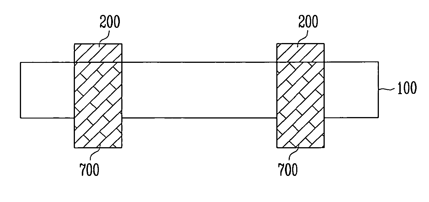
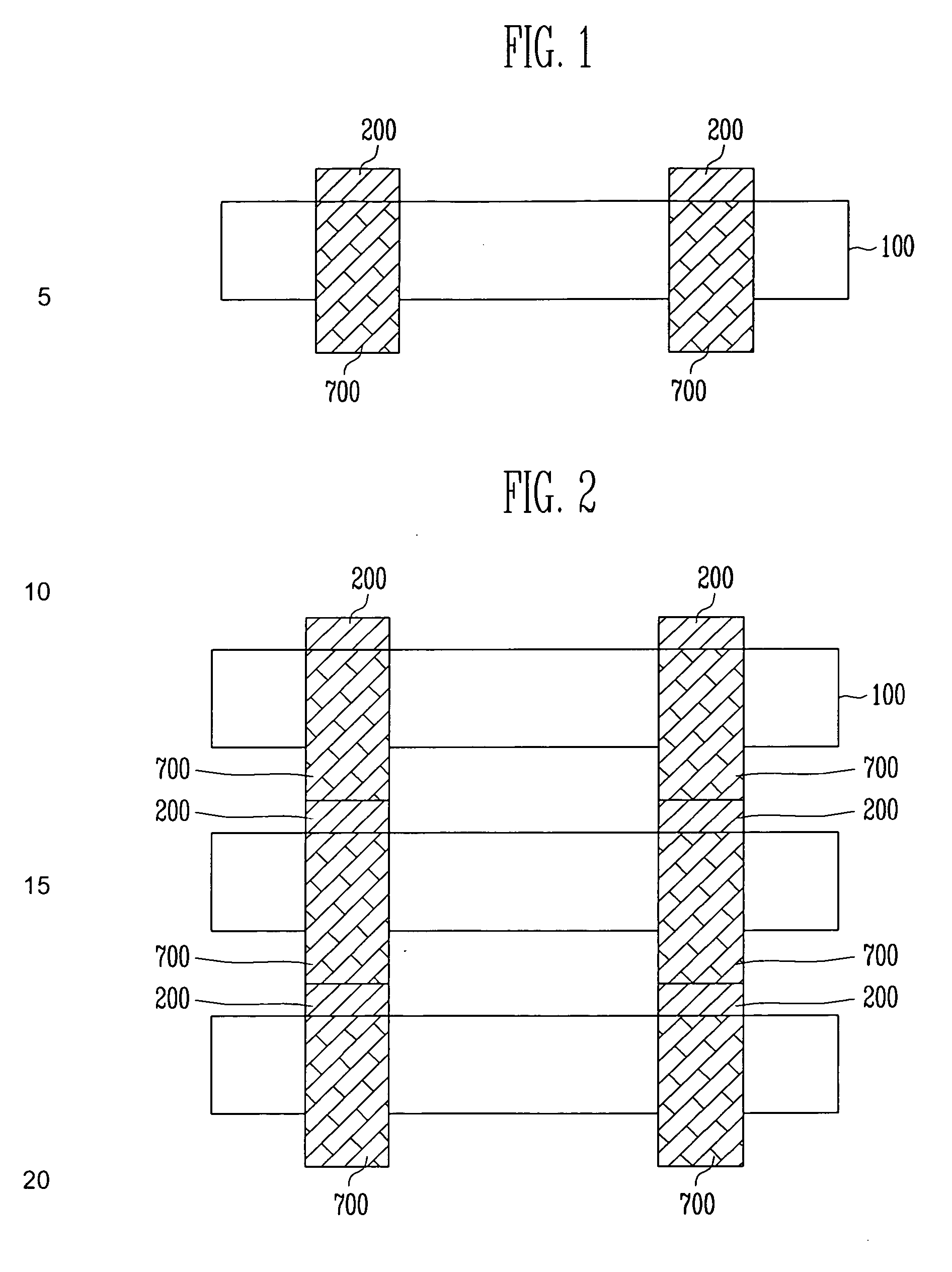
[0023]FIG. 1 is a cross-sectional view of a chip according to an exemplary embodiment of the present invention, and FIG. 2 is a cross-sectional view of a chip stack according to an exemplary embodiment of the present invention.

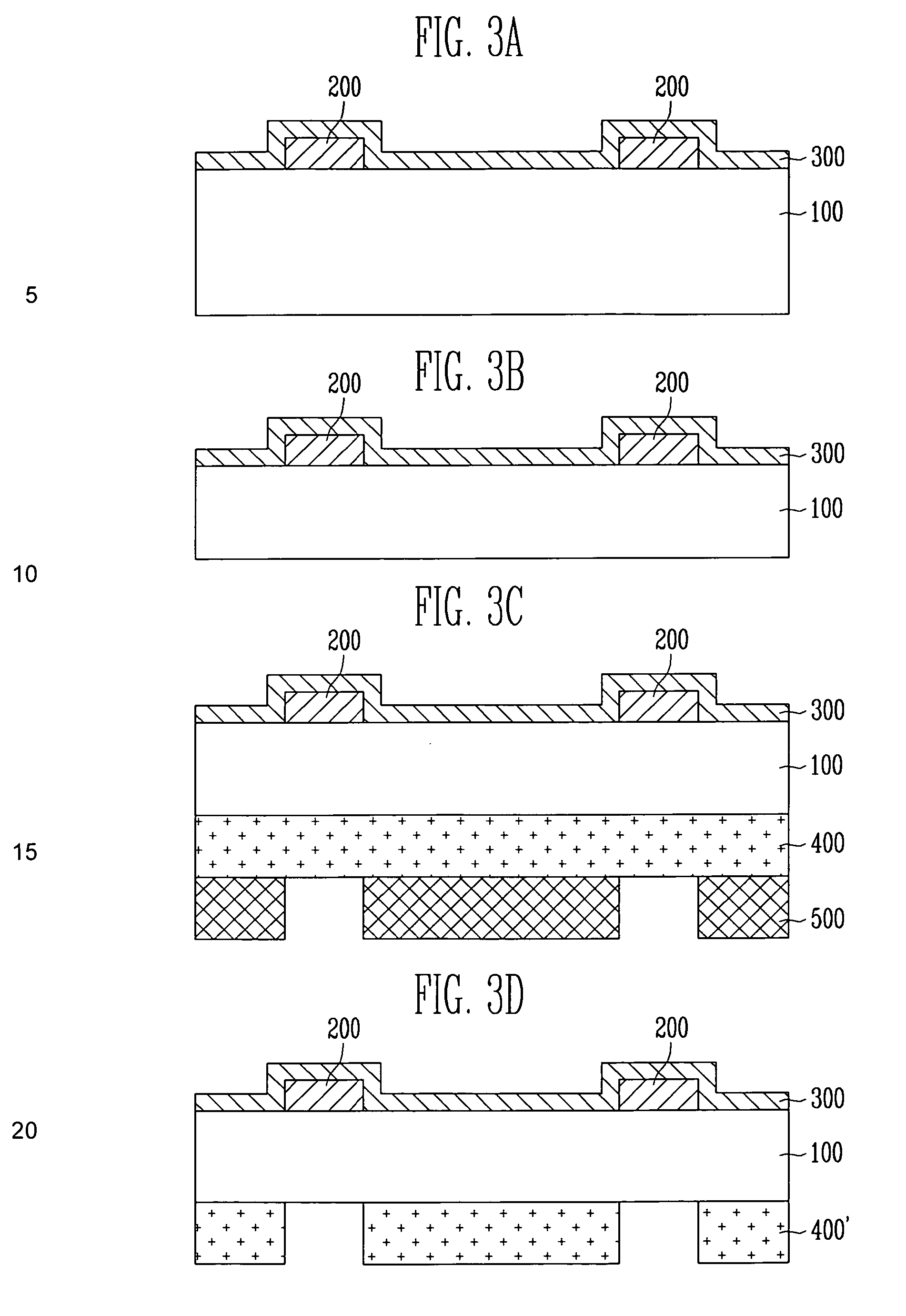
[0024] Referring to FIG. 1, the chip of the present invention comprises at least one pad 200 formed on a wafer 100, a via hole (see 600 in FIG. 3e) which penetrates the wafer to expose the bottom of the pad 200, and a metal layer 700 which protrudes from the bottom of the wafer 100 by a predetermined thickness.

[0025] Referring to FIG. 2, the chip stack of...


PUM


Abstract

Provided are a chip, a chip stack, and a method of manufacturing the same. A plurality of chips which each include: at least one pad formed on a wafer; and a metal layer which protrudes up to a predetermined thickness from the bottom of the wafer and is formed in a via hole exposing the bottom of the pad are stacked such that the pad and the metal layer of adjacent chips are bonded. This leads to a simplified manufacturing process, high chip performance and a small footprint for a chip stack.

Description

CROSS-REFERENCE TO RELATED APPLICATION [0001] This application claims priority to and the benefit of Korean Patent Application No. 2005-89724, filed on Sep. 27, 2005, the disclosure of which is incorporated herein by reference in its entirety. BACKGROUND [0002] 1. Field of the Invention [0003] The present invention relates to a chip, a chip stack, and a method of manufacturing the same, and more particularly, to a chip, a chip stack, and a method of manufacturing the same in which a chip manufacturing process is simplified, chip performance is improved, and a footprint for a chip stack is made small by forming a metal layer protruding from the bottom of a wafer up to a predetermined thickness in a via hole penetrating the wafer to expose the bottom of a pad formed on the wafer. [0004] 2. Discussion of Related Art [0005] The ongoing development of wireless communication and digital multimedia technology, coupled with increasing consumer demand, continues to fuel the trend toward mini...

Claims


Application Information

Patent Timeline
Patent Type & Authority Applications(United States)
IPC IPC(8): H01L21/44H01L21/4763
CPCH01L21/76898H01L23/481H01L25/0657H01L2224/16H01L2225/06513H01L2225/06541H01L25/50H01L2224/05573H01L2224/13025H01L2224/05568H01L2224/16146H01L24/11H01L24/13H01L24/05H01L2224/13009H01L2224/0557
Inventor JU, CHULL WONMIN, BYOUNG GUEKIM, SEONG ILLEE, JONG MINLEE, KYUNG HOKANG, YOUNG IL
Owner ELECTRONICS & TELECOMM RES INST
Why Eureka
Try Eureka