Surface treatment method after nitride material laser lift-off

A laser lift-off and surface treatment technology, used in electrical components, semiconductor/solid-state device manufacturing, circuits, etc., can solve problems such as cracking, impact on device performance and stability, hinder industrial development and promotion, and reduce cracks or chipping. The probability of cracking, the improvement of composition and roughness, the effect of good market application prospects

Active Publication Date: 2017-09-29
SINO NITRIDE SEMICON
View PDF5 Cites 7 Cited by
  • Summary
  • Abstract
  • Description
  • Claims
  • Application Information

AI Technical Summary

Problems solved by technology

[0004] Impurities such as metals remaining after the nitride semiconductor substrate is lifted off by laser and the rough surface caused by it will destroy the activity of the substrate surface in the preparation of thermal and conductive nitride composite substrates and single crystal substrates, increasing the difficulty of homoepitaxial growth. The leakage current of the device will be increased in the preparation of the structural device, which will affect the light extraction efficiency, performance and stability of the device. Therefore, it is necessary to perform corrosion treatment on the surface after laser lift-off
At present, there are two methods for surface treatment after laser lift-off in the market or scientific research institutions. 1) Heating and melting technology. The melting point of metal Ga is 29.8°C, and Ga metal can be melted and removed by heating, but heating has a negative effect on GaN epitaxial film and bonding. The combined dielectric layer has certain damage, which significantly increases the surface defects and crystal quality of the GaN thin film, and finally affects the device performance and stability. Moreover, this method is only applicable to the GaN surface after laser lift-off.
2) Hydrochloric acid immersion method, this method is suitable for surface treatment after stripping of AlN, GaN and other nitrides, this method uses hydrochloric acid immersion corrosion, then the substrate after stripping is placed in the liquid, that is, the substrate is completely immersed in the liquid, Ga, Ga, Active metals such as Al will react rapidly and violently, release a large amount of gas, and cause a very large impact on the surface of the stripped nitride, and the residual stress changes very rapidly. , AlN film cracks, or even cracks, damage the substrate surface and increase the difficulty of epitaxy, hindering the development and promotion of industrialization. In addition, hydrochloric acid immersion corrosion has a certain corrosive effect on the dielectric layer and the transfer substrate, which is easy to cause The debonding phenomenon seriously affects the stability of the bonding product and its device performance, increases the leakage current of the device and the stability of long-distance work

Method used


Image

  • Surface treatment method after nitride material laser lift-off
  • Surface treatment method after nitride material laser lift-off
  • Surface treatment method after nitride material laser lift-off

Examples


Embodiment 1

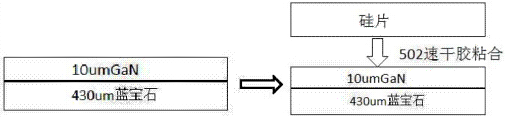
[0047] S11. Using MOCVD technology to grow a 10um-thick GaN epitaxial film on a 2-inch 430um-thick sapphire substrate to prepare a sapphire-based GaN composite substrate.

[0048] S12. Use 502 quick-drying adhesive to bond the GaN surface of the silicon wafer and the GaN composite substrate, as attached Figure 3-1 shown.

[0049] S13, using a 248nm wavelength laser to lift off the sapphire substrate, exposing the surface after laser lift off, and obtaining a GaN composite substrate.

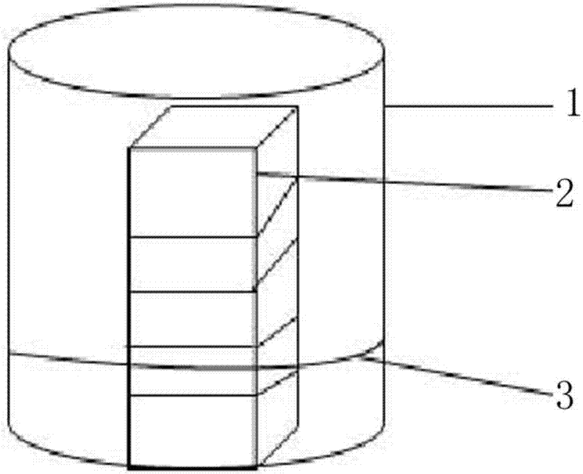
[0050] S14, choose as attached figure 1 For the chamber structure shown, put 300ml of hydrochloric acid with a concentration of 37% into the beaker, place the laser-stripped GaN composite substrate 2cm above the liquid surface at the height of the slot, and seal the opening of the beaker with tin foil. After standing still for 40 minutes, use isopropanol, acetone and ultrapure water to perform ultrasonic cleaning, and blow dry with nitrogen gas to complete the atmosphere corrosion treatment of...

Embodiment 2

[0052] S21. Using PVD to grow 25nm AlN as a buffer layer on a 2-inch 430um-thick sapphire substrate, and then using MOCVD epitaxy technology combined with HVPE epitaxy technology to prepare a 20um-thick GaN composite substrate.

[0053] S22, using 502 quick-drying adhesive to bond the quartz glass sheet and the GaN surface of the GaN composite substrate.

[0054] S23. Use a 193nm wavelength laser to lift off the sapphire substrate to expose the surface after laser lift off to obtain a GaN composite substrate, as shown in the attached Pic 4-1 shown.

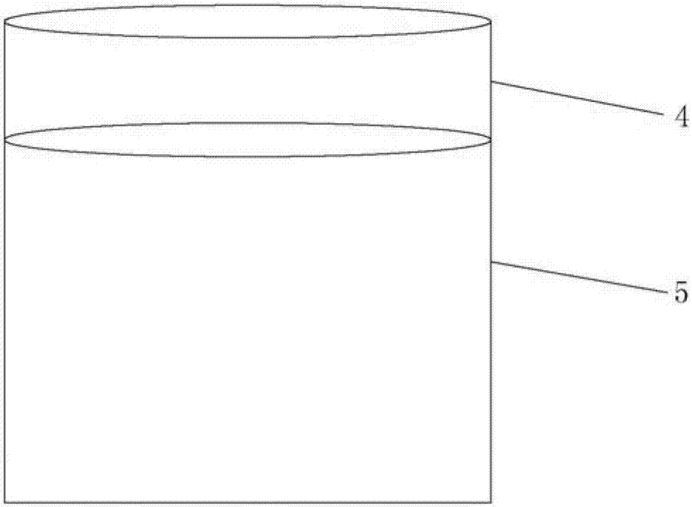
[0055] S24 option attached figure 2 In the chamber structure shown, put the GaN composite substrate into the sealed chamber, close the chamber door, let hydrochloric acid gas flow in, let it stand for 30 minutes, use isopropanol, acetone and ultrapure water to perform ultrasonic cleaning, and blow dry with nitrogen gas. That is, the atmosphere etching treatment on the laser peeled surface is completed. as attached Figure 5-...

Embodiment 3

[0057] S31. Using MOCVD technology to grow a 10um-thick GaN epitaxial film on a 2-inch 430um-thick sapphire substrate to prepare a sapphire-based GaN composite substrate.

[0058] S32. Evaporate an Au film with a thickness of 1 micron on the GaN epitaxial layer and the tungsten-copper (WCu) substrate respectively, and then bond the WCu substrate and the GaN epitaxial layer together at 300°C and a pressure of 10 tons for 120 minutes .

[0059] S33. Using the 248nm wavelength laser lift-off technology to remove the sapphire substrate to expose the surface after laser lift-off. as attached Figure 5-1 shown.

[0060] S34, choose as attached figure 2 Chamber structure shown. Place the laser-stripped GaN composite substrate in the upper and lower fixtures, and fix the fixtures. Put it into a sealed cavity, close the cavity door, let hydrochloric acid gas flow in, let it stand for 20 minutes, use isopropanol, acetone and ultrapure water to perform ultrasonic cleaning, and blow...


PUM

PropertyMeasurementUnit
melting pointaaaaaaaaaa
thicknessaaaaaaaaaa

Abstract

The invention discloses a surface treatment method after nitride material laser lift-off. The surface treatment method comprises the following steps: preparing a nitride composite substrate or a nitride single crystal substrate in a laser lift-off manner; selecting a cavity, enabling the cavity to be filled with a volatile corrosive liquid, putting the nitride composite substrate or the nitride single crystal substrate above a liquid level in the cavity, sealing the cavity so that a closed cavity is formed, standing for a period of scheduled time T, and using an atmosphere generated by volatilization of the corrosive liquid to carry out corrosion treatment on the surface, after laser lift-off, of the nitride composite substrate or the nitride single crystal substrate; cleaning and drying the nitride composite substrate or the nitride single crystal substrate in the cavity to complete atmosphere corrosion treatment on the surface after laser lift-off. A nitride surface after lift-off is treated by using an atmosphere corrosion method, the impurities such as residual metals on the surface after lift-off are removed, the ingredients and roughness of the surface after lift-off are improved, and the later-period homoepitaxy effect and chip performance are improved.

Description

technical field [0001] The invention relates to a surface treatment method after laser stripping of a nitride material. Background technique [0002] Representative materials of the third-generation semiconductor nitride materials, especially GaN and AlN materials, are all wide-bandgap semiconductors with direct band gaps of 3.39ev and 6.3ev. Detectors and electronic power devices have broad market application prospects. [0003] Due to the complex and expensive preparation process of GaN single crystal, GaN-based light-emitting diodes are generally heteroepitaxial on sapphire substrates with similar crystal structure, but sapphire is insulating and has poor thermal conductivity, which affects the life of its LED chips and The luminous efficiency leads to uneven current distribution and serious heat dissipation problems, the hardness is difficult to cleavage, and the chip process is complicated, and the material utilization rate is low, which limits its application in high ...

Claims


Application Information

Patent Timeline
Patent Type & Authority Applications(China)
IPC IPC(8): H01L21/306H01L33/00
CPCH01L21/30621H01L33/0075H01L33/0093
Inventor 汪青梁文林任俊杰罗家懋张集发童玉珍孙明张国义
Owner SINO NITRIDE SEMICON
Why Eureka
Try Eureka