Low current offset integrator with signal independent low input capacitance buffer circuit

a low-current offset, integrator technology, applied in logic circuit coupling/interface arrangement, time-delay network, pulse technique, etc., can solve the problem of input current offset error, etc. problem

Active Publication Date: 2008-06-10
NAT SEMICON CORP
View PDF8 Cites 17 Cited by
  • Summary
  • Abstract
  • Description
  • Claims
  • Application Information

AI Technical Summary

Problems solved by technology

One factor that affects the accuracy of a current input ADC is the input current offset error.
There are typically multiple sources of errors that contribute to the ADC's input current offset error.
For instance, circuitry outside of the ADC circuit, such as the electro static discharge (ESD) circuit can introduce input current offset error.
However, the dominant error source is usually the injection of non-zero charge packets by active device switches in the integrator circuit used to reconfigure the modulator throughout different clock phases to carry out the different operational functions.

Method used


Image

  • Low current offset integrator with signal independent low input capacitance buffer circuit
  • Low current offset integrator with signal independent low input capacitance buffer circuit
  • Low current offset integrator with signal independent low input capacitance buffer circuit

Examples


Embodiment Construction

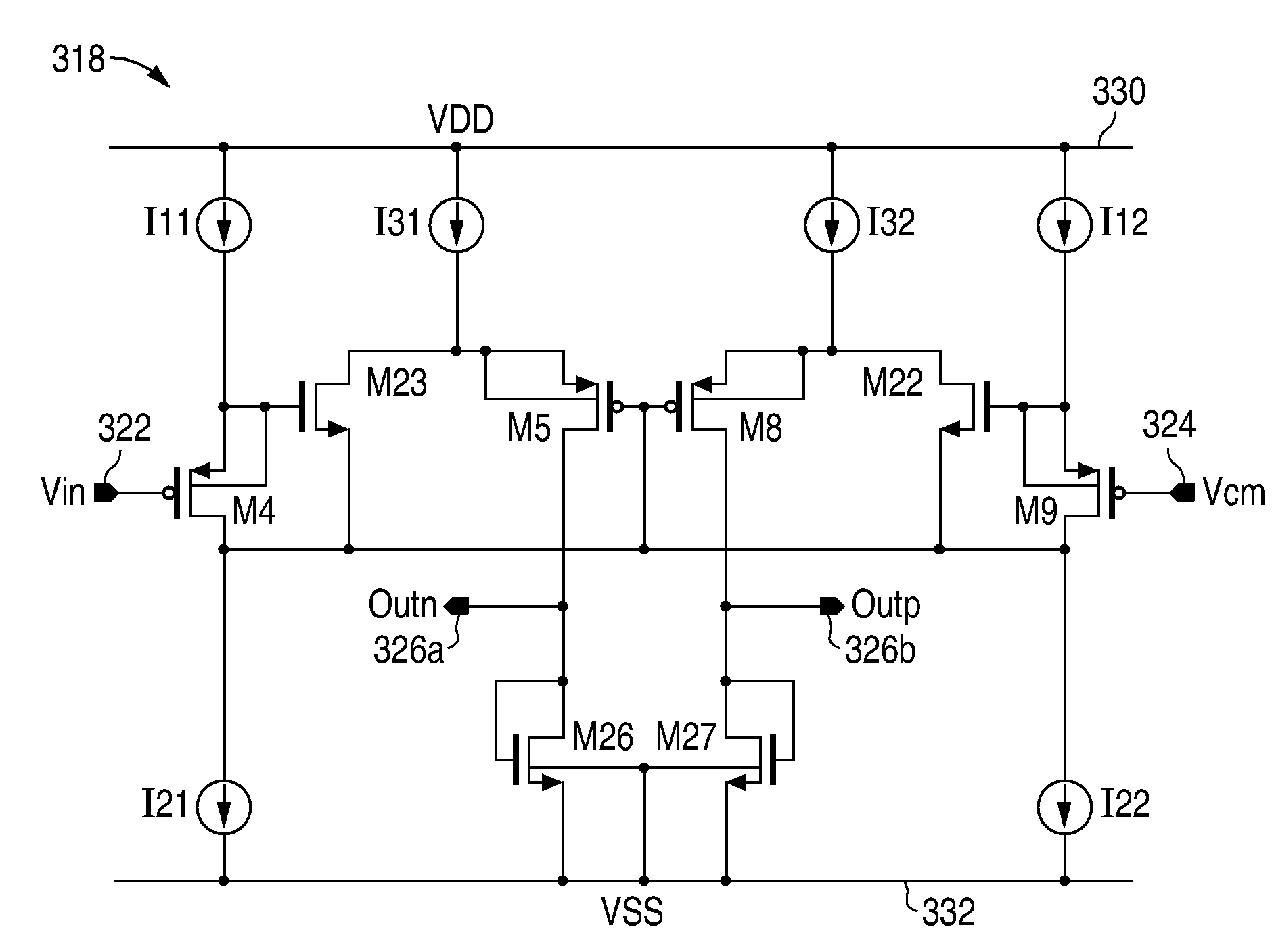
[0016]In accordance with the principles of the present invention, a buffer circuit with signal-independent low input capacitance uses bootstrapping techniques at the input device so that the channel region of the input device is insensitive to the absolute input voltage at the gate of the input device. Furthermore, bootstrapping techniques are used to establish local feedback paths to greatly reduce the input capacitance at the input device. The advantages of the buffer circuit are that both the magnitude and the variance of the input capacitance of the buffer circuit are decreased by several orders of magnitude over conventional devices.

[0017]In particular, the low input capacitance buffer circuit of the present invention has particular application in analog-to-digital converters (ADCs), especially in current input ADCs receiving a low level input current to be digitized. The buffer circuit of the present invention can be coupled to an integrator to form a charge balancing modulato...


PUM


Abstract

A buffer circuit (318) including a first half circuit and a second half circuit. Each half circuit includes a first MOS transistor (M4, M9) as the input device and a source follower, a second MOS transistor (M23, M22) as a transconductance amplifier device, and a third MOS transistor (M5, M8) as a folded cascode device. The first half circuit receives a buffer input voltage as the input voltage and the second half circuit receives a reference voltage as the input voltage. The first and second half circuits providing a pair of differential output signals indicative of the buffer input voltage. The buffer circuit has a very low input capacitance where the input capacitance does not vary with the buffer input voltage and other operating conditions, such as fabrication process, temperature and power supply voltage variations.

Description

CROSS-REFERENCE TO RELATED APPLICATIONS[0001]This application is related to the following commonly assigned and concurrently filed U.S. patent application Ser. No. 11 / 679,070, entitled “Charge Balancing Method in a Current Input ADC,” of Jun Wan and Peter R. Holloway, which patent application is incorporated herein by reference in its entirety.FIELD OF THE INVENTION[0002]The invention relates to a buffer circuit and, in particular, to a buffer circuit for use with an integrator to form a charge balancing modulator for a current input analog-to-digital converter.DESCRIPTION OF THE RELATED ART[0003]Analog-to-digital converters are used in converting or digitizing an analog input signal to generate a digital output signal indicative of the value of the analog input signal within a given conversion time. A current input ADC refers to an ADC that receives a low level input current as the analog input signal to be digitized. Current input ADCs are sometimes referred to as Coulomb-meters b...

Claims


Application Information

Patent Timeline
Patent Type & Authority Patents(United States)
IPC IPC(8): H03K19/094H03H11/26
CPCH03F3/45179H03F3/45475H03F3/45766H03F3/70H03F2200/264H03F2203/45038H03F2203/45166H03F2203/45212H03F2203/45354H03K19/0175
Inventor WAN, JUNHOLLOWAY, PETER R.
Owner NAT SEMICON CORP
Why Eureka
Try Eureka