Electro-optical device, method of manufacturing the same, and electronic apparatus

a manufacturing method and electronic technology, applied in non-linear optics, identification means, instruments, etc., can solve the problems of deterioration of breakdown voltage performance, subject of electronic optical devices according to the related art technology, etc., to simplify manufacturing processes and avoid damage

Active Publication Date: 2008-06-17
SEIKO EPSON CORP
View PDF12 Cites 10 Cited by
  • Summary
  • Abstract
  • Description
  • Claims
  • Application Information

AI Technical Summary

Benefits of technology

[0009]In order to satisfy these requirements, the first electrodes and the second electrodes may be formed to have the same area. Thus, it is possible to reduce or prevent the portions of the electrodes that do not face the electrodes on the other side, that is, surplus portions that do not function in the storage capacitors, from occupying the limited area on the substrate. On the other hand, since both electrodes face each other with no wasted portion, it is possible to achieve reduction and minuteness in size of the electro-optical device, and to prevent the capacitance from being reduced.
[0074]Since the electronic apparatus of exemplary embodiments of the present invention includes the above described electro-optical device having the storage capacitors which exhibit an excellent breakdown-voltage performance, it is possible to realize various electronic apparatuses, such as a projection-type display device, a liquid crystal TV, a mobile telephone, an electronic pocketbook, a word processor, a viewfinder-type or monitor-direct-view-type video tape recorder, a workstation, a videophone, a POS terminal, and a touch panel, capable of displaying high quality images.

Problems solved by technology

However, the electro-optical device according to the related art technology is subject to the following problems.
Even if the first electrodes and the second electrodes are not short circuited, electrostatic focusing may occur in the end due to the remnants, to deteriorate a breakdown-voltage performance.

Method used


Image

  • Electro-optical device, method of manufacturing the same, and electronic apparatus
  • Electro-optical device, method of manufacturing the same, and electronic apparatus
  • Electro-optical device, method of manufacturing the same, and electronic apparatus

Examples


Embodiment Construction

[0095]Exemplary embodiments of the present invention will now be described with reference to the drawings. According to the exemplary embodiment, an electro-optical device according to the present invention is applied to a liquid crystal device.

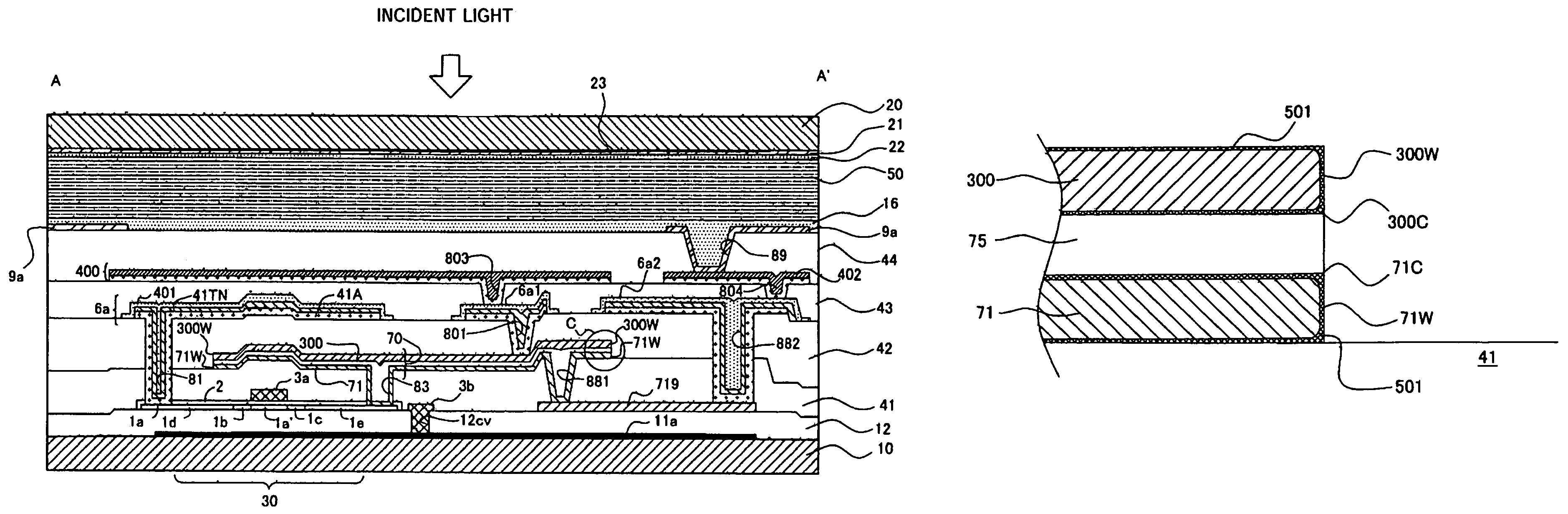
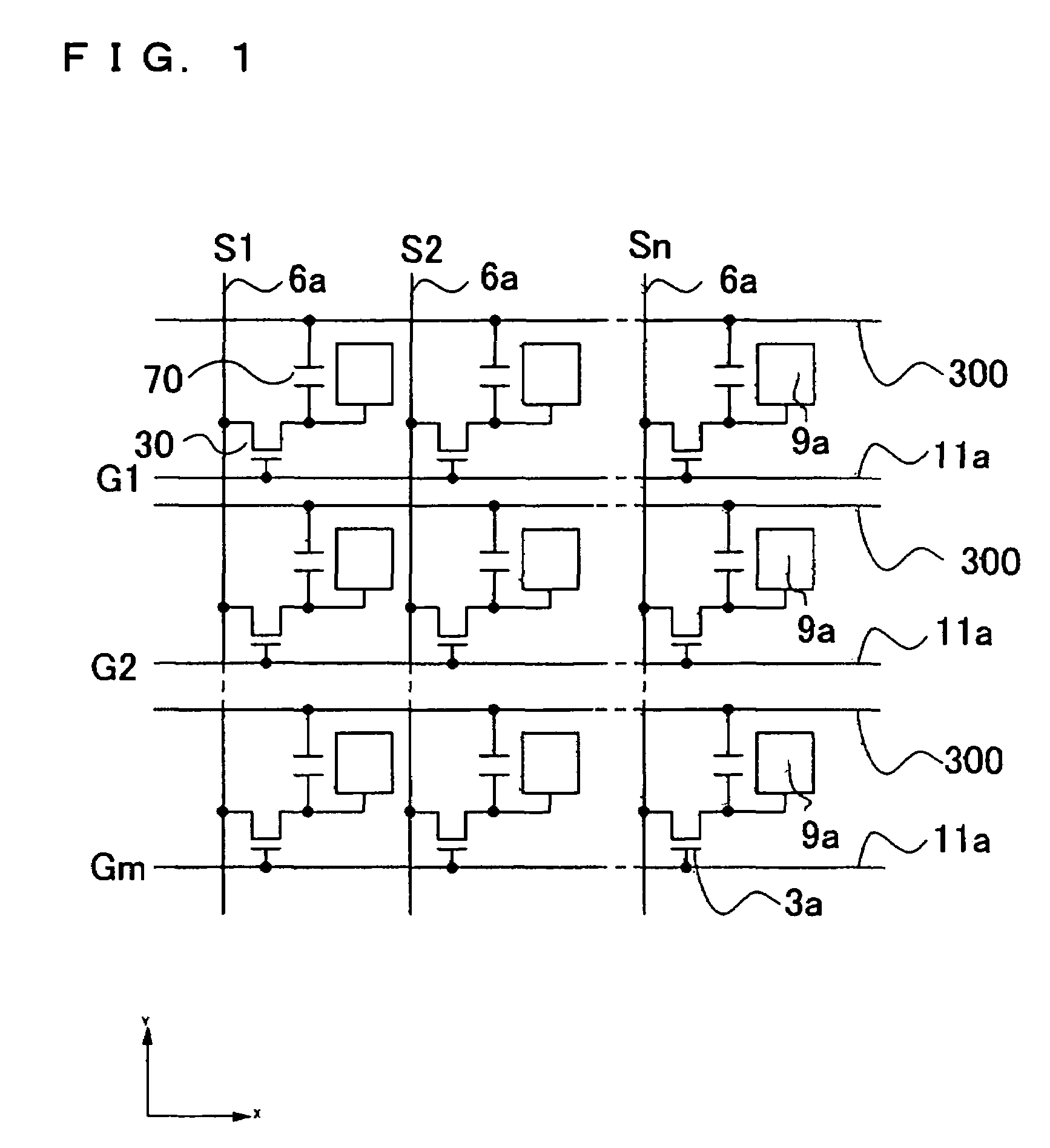
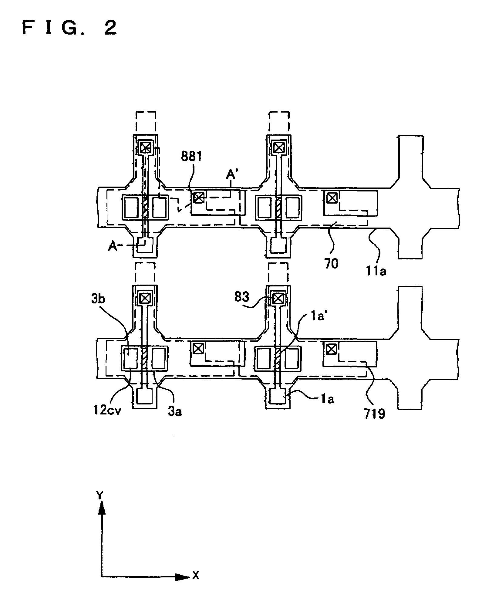
[0096]The structure of a pixel portion of an electro-optical device according to an exemplary embodiment of the present invention will now be described with reference to FIGS. 1 to 4. Here, FIG. 1 is a schematic that shows an equivalent circuit of various elements, wiring lines, etc. in a plurality of pixels formed in a matrix that constitutes an image display region of the electro-optical device. FIGS. 2 and 3 are schematics that show plan views of a plurality of pixel groups adjacent to each other on a TFT array substrate on which data lines, scanning lines, and pixel electrodes are formed. Also, FIGS. 2 and 3 respectively illustrate a lower portion (FIG. 2) and an upper portion (FIG. 3) in a laminated structure to be described later. FIG. ...


PUM

PropertyMeasurementUnit
thicknessaaaaaaaaaa
thicknessaaaaaaaaaa
temperatureaaaaaaaaaa

Abstract

Exemplary embodiments of the present invention include an electro-optical device including storage capacitors having excellent breakdown-voltage performance to function properly. Exemplary embodiments further include an electro-optical device including data lines, scanning lines, thin film transistors, and pixel electrodes formed on a substrate. The electro-optical device also includes storage capacitors composed of first electrodes electrically connected to the thin film transistors and the pixel electrodes, second electrodes that are arranged to face the first electrodes, and dielectric films arranged between the first electrodes and the second electrodes, and oxidation films obtained by oxidizing part or all of the surfaces of at least one of the first electrodes and the second electrodes.

Description

BACKGROUND OF THE INVENTION[0001]1. Field of Invention[0002]The present invention relates to electro-optical devices such as an active-matrix-driving liquid crystal device, an electrophoresis device such as electronic paper, an electro-luminescent (EL) display device, and a device including an electron emission element such as a field emission display and a surface-conduction electron-emitter display, and to a method for manufacturing the same. Also, the present invention relates to electronic apparatus including the electro-optical device.[0003]2. Description of Related Art[0004]The related art includes electro-optical devices capable of active-matrix-driving. The related art electro-optical devices include pixel electrodes arranged on a substrate in a matrix, thin film transistors (TFT) connected to each of the pixel electrodes, and data lines and scanning lines connected to the TFTs and provided in parallel in column and row directions.[0005]The electro-optical device of the rela...

Claims


Application Information

Patent Timeline
Patent Type & Authority Patents(United States)
IPC IPC(8): H01L27/14G02F1/136G02F1/1368G02F1/1362G09F9/00G09F9/30H01L51/50
CPCG02F1/136213G02F1/136
Inventor FUKUHARA, KEIJIKAWAKAMI, YASUSHI
Owner SEIKO EPSON CORP
Why Eureka
Try Eureka