Writing and reading of data in probe-based data storage devices

a data storage device and probe-based technology, applied in the direction of digital signal error detection/correction, coding, instruments, etc., can solve the problems of variable types of errors that can be encountered in the probe-based storage device, and achieve the effect of reducing the likelihood of errors preventing the correct recovery of codewords, minimizing the number of bytes, and maximal byte spacing

Inactive Publication Date: 2008-06-17
INT BUSINESS MASCH CORP
View PDF8 Cites 5 Cited by
  • Summary
  • Abstract
  • Description
  • Claims
  • Application Information

AI Technical Summary

Benefits of technology

[0015]Successive bytes of each sub-block are selected cyclically from the r codewords. Hence bytes from the same codeword are always r bytes apart in each sub-block. Since each sub-block is then written to a different storage field of the array, bytes from the same codeword are always r-bytes apart in each storage field. This gives the maximum spacing of bytes from individual codewords in all storage fields, reducing the likelihood of errors preventing correct recovery of the codewords, and hence the original user block. In particular, the distribution of codewords across the A storage fields, and maximal byte-spacing for individual codewords in each storage field, minimizes the number of bytes from any given codeword that are likely to be affected by localized damage to the storage surface.
[0016]In addition, since bytes are written sequentially by the probe in a given storage field, bytes from the same codeword are only written once every r-bytes, thereby reducing the effect of errors due to temporary abnormalities such as shocks. Moreover, by appropriate selection of the values of r and C in the coding process, the system can be employed with any array size A and can accommodate any size of user data block. Methods embodying this aspect of the invention thus exploit the inherent parallelism of the probe-based array to provide an efficient and flexible system for writing user data blocks with a high degree of tolerance to errors.
[0026]Thus, methods embodying this aspect of the invention exploit the concept of sub-arrays to allow read / write operations to be performed at variable rates. This allows probe-based storage devices to accommodate differing data rates of a number of different interfaces with which data may be exchanged in operation. Data written at different rates can coexist on the storage surface, and stored data can be read back at any of the available read-rates, regardless of the rate at which that data was originally written. As a result, embodiments of this aspect of the invention offer highly flexible probe-based storage systems.

Problems solved by technology

Various types of errors can be encountered in probe-based storage devices.
These errors are typically related to surface damage such as scratches in the storage surface, to noise or to abnormal conditions during the read / write process, e.g. vibrations due to external shocks.

Method used


Image

  • Writing and reading of data in probe-based data storage devices
  • Writing and reading of data in probe-based data storage devices
  • Writing and reading of data in probe-based data storage devices

Examples


example 1

[0070]Physical array size A=4096 storage fields; user block size=576 bytes; r=4; Ad=512 storage fields; As=16 storage fields; k0=512 / 16=32; k1=576 / 16=36; and k2=4096 / 512=8.

example 2

[0071]Physical array size A=4096 storage fields; user block size=576 bytes; r=4; Ad=512 storage fields; As=32 storage fields; k0=512 / 32=16; k1=576 / 32=18; and k2=4096 / 512=8.

example 3

[0072]Physical array size A=4096 storage fields; user block size=4096 bytes; r=16; Ad=512 storage fields; As=32 storage fields; k0=512 / 32=16; k1=4096 / 32=128; and k2=4096 / 512=8.

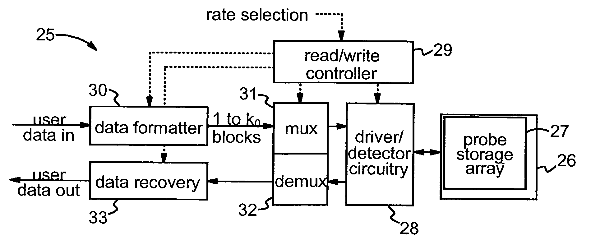
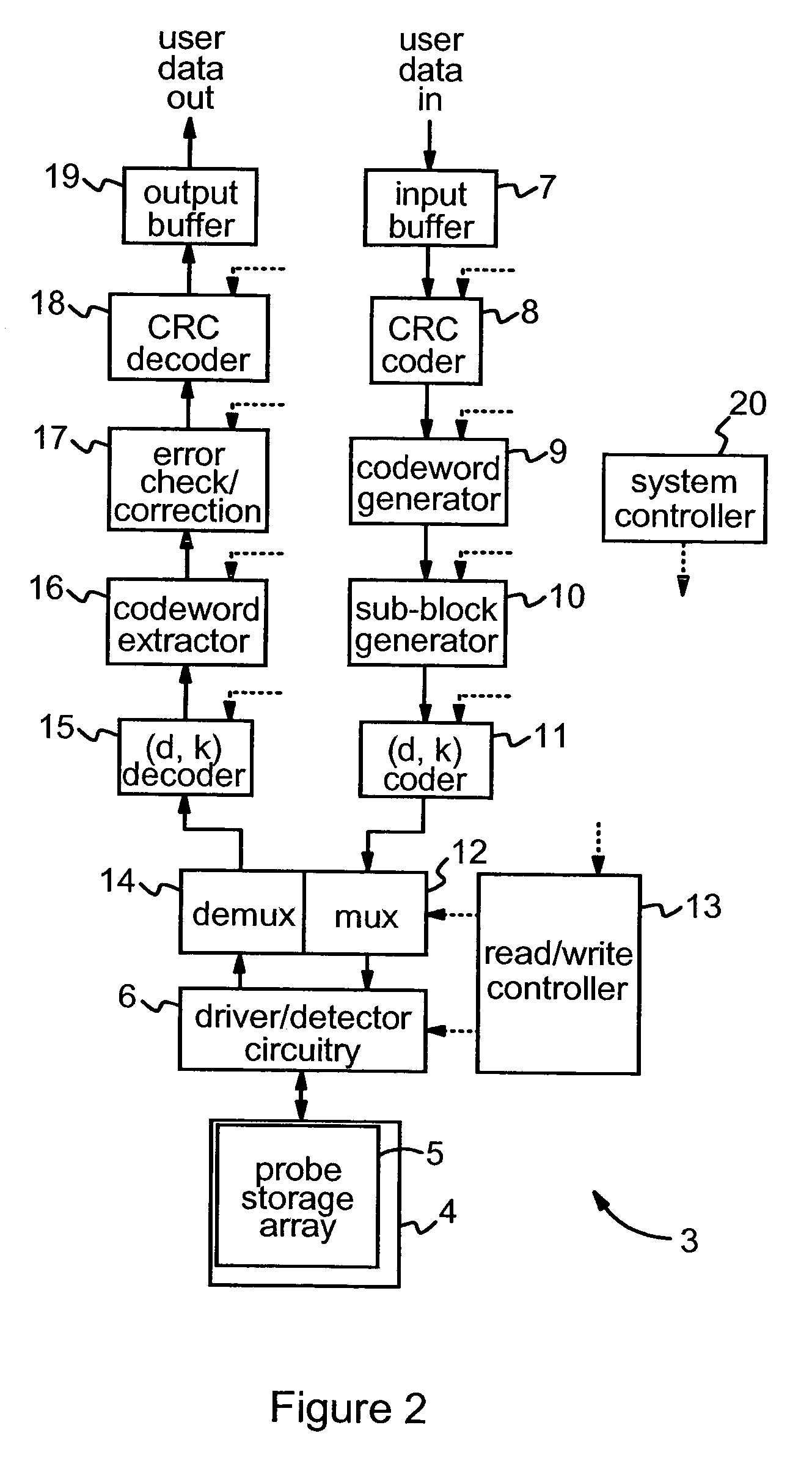
[0073]It will be appreciated that the read / write control systems of embodiments of the invention can support various host interfaces for probe-based storage devices having various array and storage field sizes, and provide tolerance to various types of errors. Independent write and read rates, as well as variations in these rates, are supported. Embodiments of the invention can be employed with any probe-storage array, regardless of the particular probe technology and array addressing scheme employed. It will of course be appreciated that, while preferred embodiments have been described in detail above, many changes and modifications can be made to the embodiments described without departing from the scope of the invention.


PUM


Abstract

Methods and apparatus are provided for controlling writing and reading of data in an array of A storage fields of a probe-based data storage device in which data is written to and read from the array of storage fields by a corresponding array of probes. One method provides error-tolerance by exploiting the inherent parallelism of the probe storage array. A user data block to be written to the A-field array is first coded to produce a plurality of C-byte codewords, such that r.C=k1.A where r is the number of codewords and k1 is an integer≧1. A sub-blocks of k1 bytes are produced from the codewords by selecting successive bytes of each sub-block cyclically from the r codewords. The A sub-blocks are then written via respective probes to the corresponding storage fields of the storage field array.

Description

CROSS-REFERENCE TO RELATED APPLICATIONS[0001]This application claims priority under 35 U.S.C. Section. 119 to EPO Application No. 03405698.6 filed on Sep. 26, 2003, in the European Patent Office (EPO), the entire contents of which are incorporated herein by reference.STATEMENT REGARDING FEDERALLY SPONSORED-RESEARCH OR DEVELOPMENT[0002]Not Applicable.INCORPORATION BY REFERENCE OF MATERIAL SUBMITTED ON A COMPACT DISC[0003]Not Applicable.FIELD OF THE INVENTION[0004]This invention relates generally to probe-based data storage devices. Particular embodiments of the invention provide methods and apparatus for controlling data write and read processes in such devices.BACKGROUND OF THE INVENTION[0005]In probe-based data storage devices, stored data is represented on a storage surface by the presence and absence of indentations, or ‘pits’, which are formed in the surface by a probe of the device. One example of such a device, based on the AFM (Atomic Force Microscope), is detailed in IBM Jou...

Claims


Application Information

Patent Timeline
Patent Type & Authority Patents(United States)
IPC IPC(8): H03M13/00
CPCB82Y10/00G06F11/1076G11B9/14G11B20/18G06F2211/1042G11B9/1445
Inventor ALBRECHT, THOMASANTONAKOPOULOS, THEODORECHERUBINI, GIOVANNIDHOLAKIA, AJAYELEFTHERIOU, EVANGELOS S.POZIDIS, CHARALAMPOS
Owner INT BUSINESS MASCH CORP
Why Eureka
Try Eureka