Light emitting device with phosphor wavelength conversion

a technology of light emitting devices and wavelength conversion, which is applied in the direction of semiconductor devices for light sources, discharge tubes luminescnet screens, lighting and heating apparatus, etc., can solve the problems of significant change in the correlated color temperature (cct) and/or intensity of light emitted by the device, and achieve the effect of reducing water absorption, reducing phosphor degradation, and eliminating phosphor degradation

Inactive Publication Date: 2010-07-01
INTEMATIX
View PDF99 Cites 87 Cited by
  • Summary
  • Abstract
  • Description
  • Claims
  • Application Information

AI Technical Summary

Benefits of technology

[0008]The present embodiments arose in an endeavor to provide a light emitting device which at least in part overcomes the limitations of the known arrangements and in particular, although not exclusively, reduce phosphor degradation in dev

Problems solved by technology

A problem with existing light emitting devices, in particular white light emitting devices intended for general lighting which require a high intensity output of ≈500-600 lumens or higher (i.e. an input power o

Method used


Image

  • Light emitting device with phosphor wavelength conversion
  • Light emitting device with phosphor wavelength conversion
  • Light emitting device with phosphor wavelength conversion

Examples


first embodiment

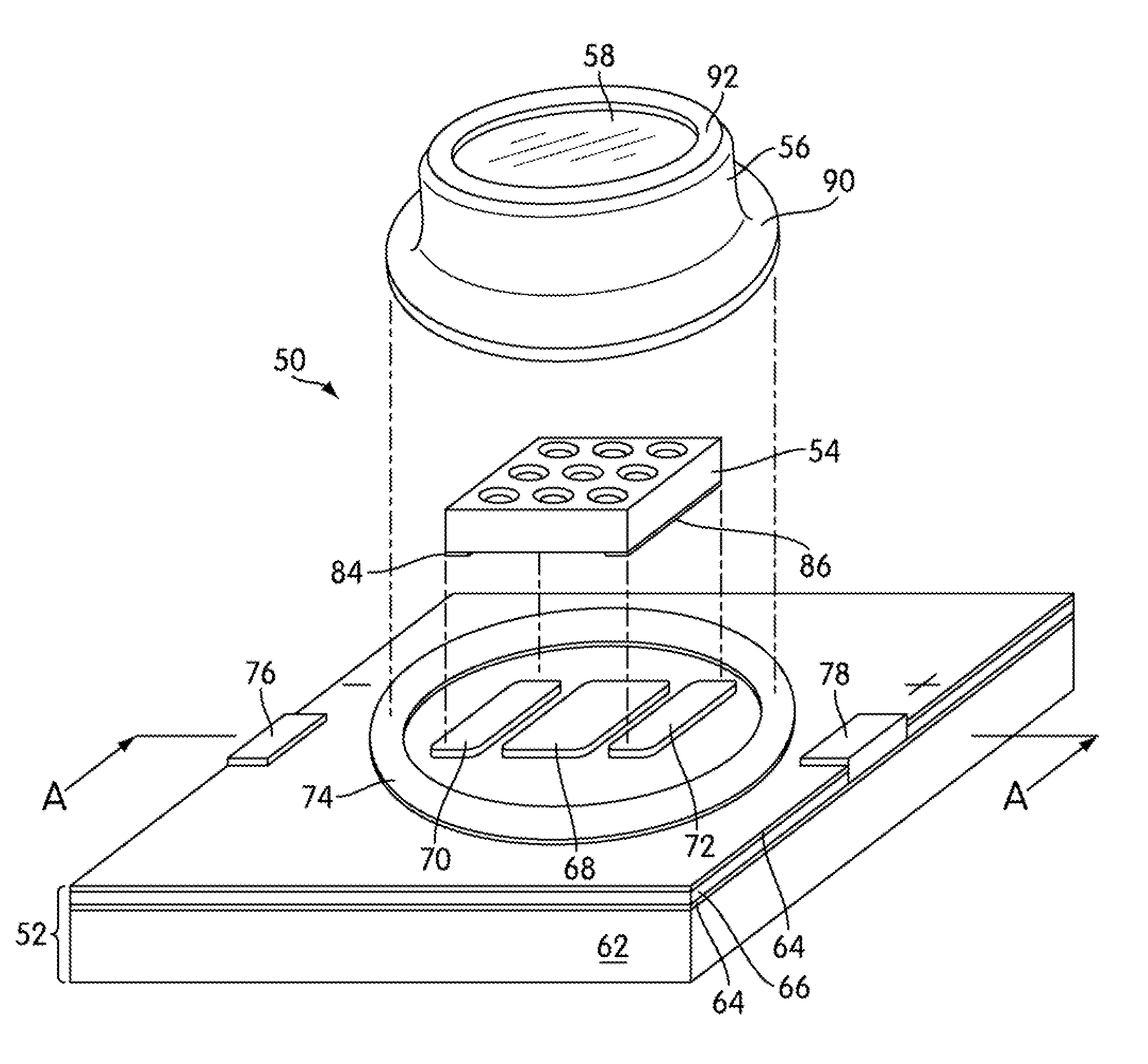
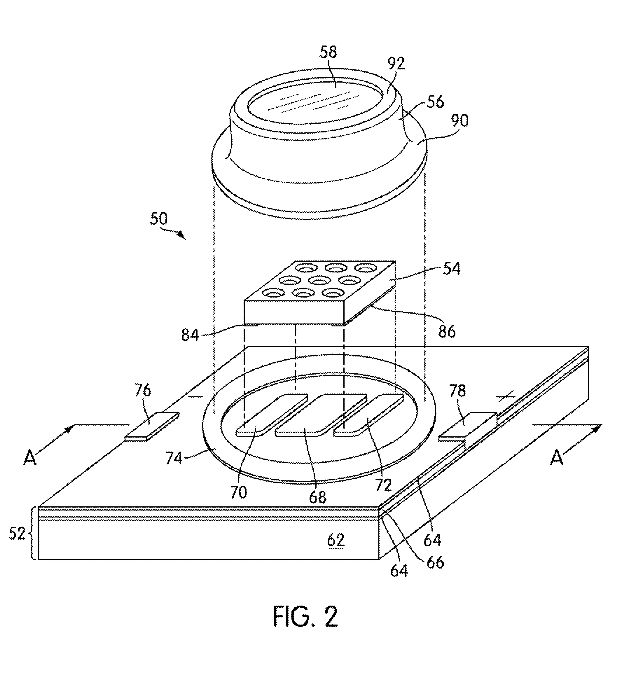
[0032]A light emitting device 50 in accordance with the invention will now be described with reference to FIGS. 2 and 3 of the accompanying drawings. The device 50 is configured to generate white light with a specific correlated color temperature (CCT) for example 2700K and an emission intensity of ≧250 lumens (i.e. ≧3 W input power) preferably ≧500-600 lumens (i.e. ≧6 W input power). The device is intended for general lighting applications such as a replacement for an incandescent, fluorescent or cold cathode fluorescent light source. It will be appreciated that the device of the present invention is not limited to such applications, emission colors or emission intensities.

[0033]Referring to FIGS. 2 and 3 the device 50 comprises a thermally conducting substrate 52 such as for example a metal core printed circuit board (MCPCB); a packaged LED array 54; a hollow metal housing (can) 56; a light transmissive (transparent) window 58 and a layer of one or more phosphor materials 60 on th...

second embodiment

[0052]Referring to FIG. 4 there is shown a schematic sectional representation of a light emitting device 50 in accordance with the invention in which a single light transmissive cover 102 is used in place of the housing / window 56 / 58 assembly. The cover 102 preferably comprises a glass such as a silica glass or quartz glass or a light transmissive inorganic material such as transparent alumina (Al2O3). The phosphor material(s) 60 is / are provided as a uniform layer over the inner surface of the cover 102. A metallization layer 104, comprising for example copper (Cu), nickel (Ni) or chromium (Cr), can be provided on at least the base of the cover 102 to enable the cover 102 to be soldered 94 or otherwise attached to the mounting pad 74. An advantage of using a single glass cover member 102 is that only a single seal 94 with the substrate 52 is required.

third embodiment

[0053]FIG. 5 is a schematic sectional representation of a light emitting device 50 in accordance with the invention. In this embodiment the glass cover member 102 comprises a substantially hemispherical (dome shaped) shell. To maximize light emission from the device 50 a metallization 106 can be provided on the interior surface of the cover member 102 that extends from the base of the cover. As shown in FIG. 5 individual LED chips 83 are mounted in direct thermal communication with the MCPCB 52 rather than a packaged array of LEDs—that is a chip-on-board (COB) arrangement.

[0054]FIG. 6 shows a schematic sectional representation of a light emitting device 50 in accordance with a forth embodiment of the invention in which the housing 56 is configured in the form of a parabolic reflector and is generally dish-shaped in form. As in other embodiments, the housing 56 is attached to the MCPCB (substrate) 52 to form a water tight, preferably air / gas tight, seal. In the embodiment illustrated...


PUM

PropertyMeasurementUnit
Luminous fluxaaaaaaaaaa

Abstract

A light emitting device comprises: a thermally conductive substrate (MCPCB); at least one LED mounted in thermal communication with a surface of the substrate; a housing attached to the substrate and configured such the housing and substrate together define a volume that totally encloses the at least one LED, the housing comprising at least a part that is light transmissive (window); and at least one phosphor material provided on an inner surface of the housing within said volume said phosphor being operable to absorb at least a part of the excitation light emitted by the at least one light emitting diode and to emit light of a second wavelength range. The housing is attached to the substrate such that the volume is substantially water tight, preferably air/gas tight.

Description

CROSS-REFERENCE TO RELATED APPLICATIONS[0001]This application claims the benefit of priority to U.S. Provisional Application 61 / 141,948, filed Dec. 31, 2008, by Yi-Qun Li et al. entitled “Light emitting device with phosphor wavelength conversion”, the specification and drawings of which are incorporated herein by reference.BACKGROUND OF THE INVENTION[0002]1. Field of the Invention[0003]This invention relates to light emitting devices with phosphor wavelength conversion and in particular, although not exclusively, to white light generating devices based on one or more light emitting diodes (LEDs). Moreover embodiments of the invention concern packaging arrangements for high emission intensity (i.e. ≧50 lumens light emission intensity or ≧1 W input power) white light emitting devices for general lighting applications.[0004]2. Description of the Related Art[0005]White light emitting LEDs (“white LEDs”) are a relatively recent innovation and offer the potential for a whole new generatio...

Claims


Application Information

Patent Timeline
IPC IPC(8): H01J1/00
CPCF21S10/02F21V7/0008F21V7/22H01L33/507H05B33/0857F21V7/06H01L33/504H01L2224/48091H01L2224/49107H01L2924/00014F21Y2115/10F21V7/30
Inventor LI, YI-QUNYANG, HAITAO
Owner INTEMATIX
Why Eureka
Try Eureka