Charge balance field effect transistor

a charge balance and transistor technology, applied in the direction of semiconductor devices, semiconductor/solid-state device details, electrical apparatus, etc., can solve the problems of charge imbalance, reduced breakdown voltage, and difficult to achieve fine dimensions

Active Publication Date: 2008-07-01
SEMICON COMPONENTS IND LLC
View PDF17 Cites 88 Cited by
  • Summary
  • Abstract
  • Description
  • Claims
  • Application Information

AI Technical Summary

Problems solved by technology

Implementing such a charge balance device structure for low voltage MOSFET has proved difficult because of process and material variations resulting in an imbalance in the carrier types which in turn cause reduced breakdown voltage.
These fine dimensions are difficult to achieve considering all the features that must fit within the cell architecture such as the heavy body junction needed for avalanche ruggedness.
For low voltage devices, each of these methods may suffer from process variations that result in charge imbalance and a relatively wide distribution in the performance features including RSP, QGD, and BVDSS.

Method used


Image

  • Charge balance field effect transistor
  • Charge balance field effect transistor
  • Charge balance field effect transistor

Examples


Embodiment Construction

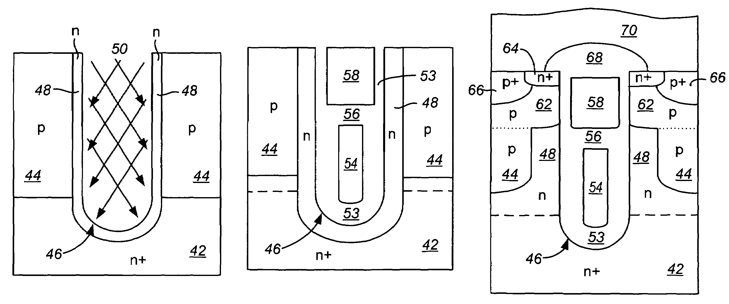
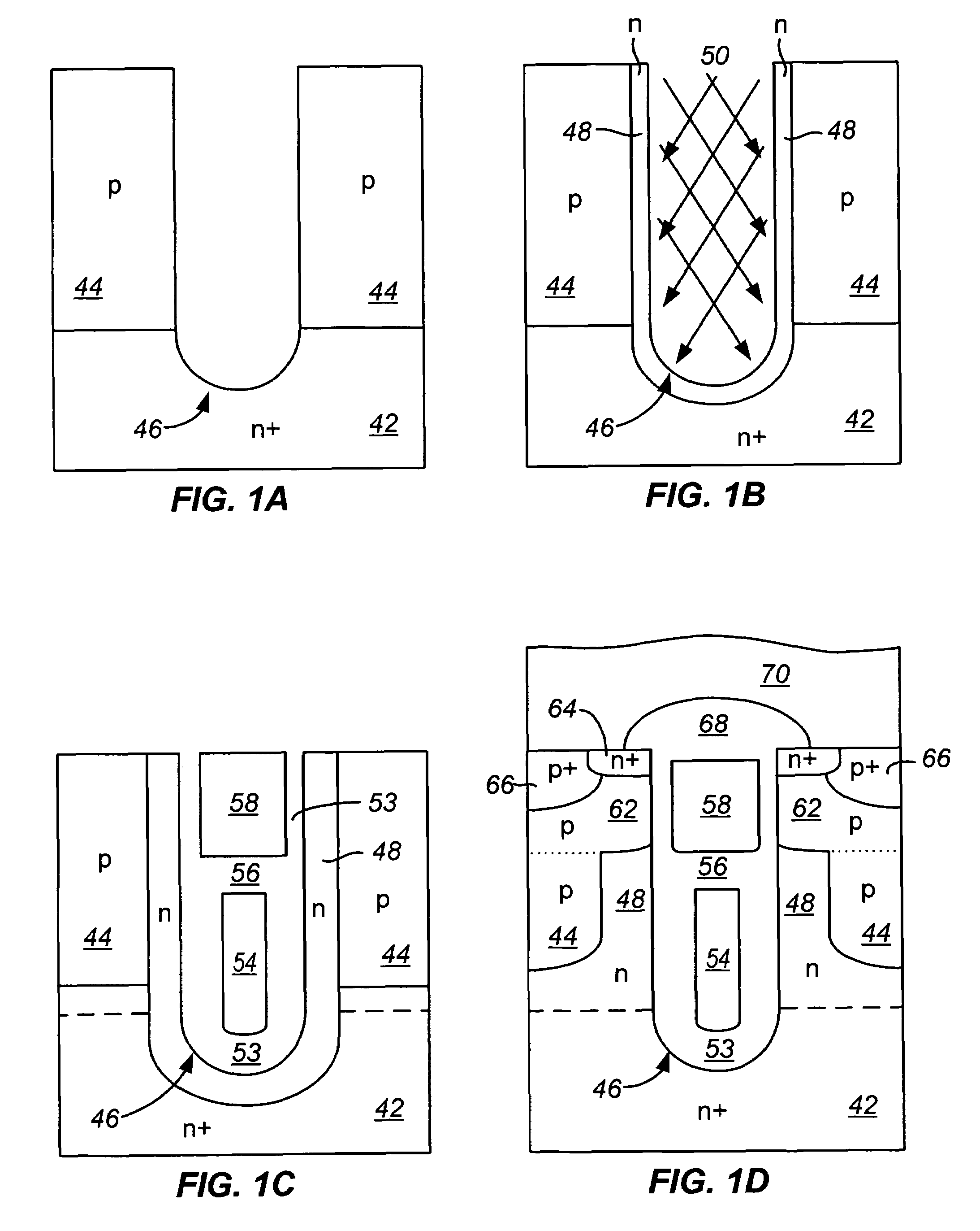
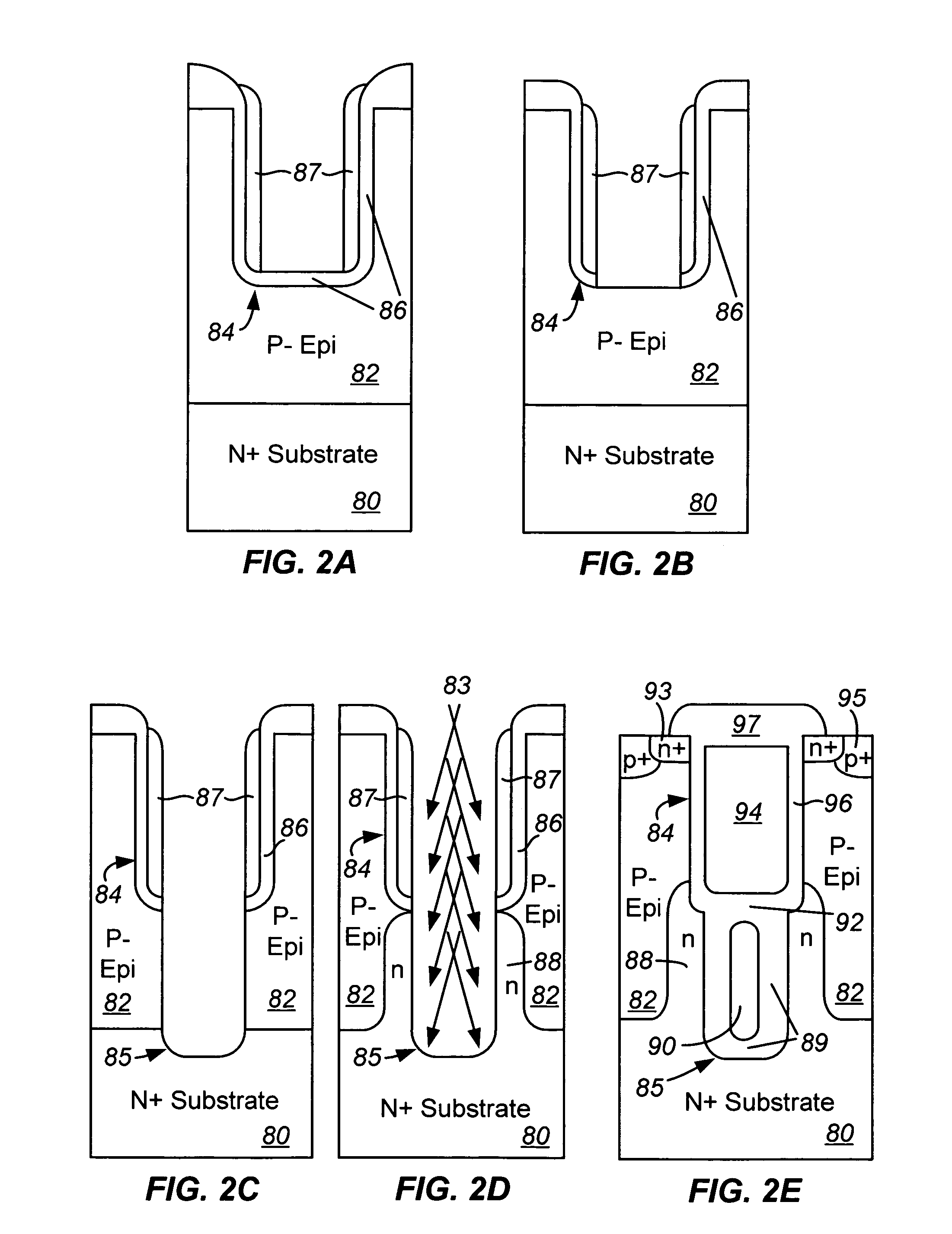
[0036]In accordance with an embodiment of the present invention, an n-channel shielded gate MOSFET, which is particularly useful for low voltage applications but not limited thereto, is formed in a p-type epitaxial layer rather than the conventional n-type epitaxial layer. This provides opportunities to simplify the process, such as eliminating the process steps associated with forming the p-type body region.

[0037]FIGS. 1A-1D are simplified cross section views illustrating a process sequence for forming a charge balance MOSFET according to an embodiment of the present invention. In FIG. 1A, a p-type epitaxial layer 44 is formed (e.g., by selective epitaxial growth of silicon) over a silicon substrate 42. In one embodiment, the starting wafer material includes substrate 42 and its overlying p-type epitaxial layer 44. A convention trench etch is carried out to form trench 46 extending through epitaxial layer 44 and terminate is substrate 42. An optional anneal step may then be perform...


PUM

PropertyMeasurementUnit
conductivity typeaaaaaaaaaa
conductivityaaaaaaaaaa
voltageaaaaaaaaaa

Abstract

A field effect transistor is formed as follows. A semiconductor region of a first conductivity type with an epitaxial layer of a second conductivity extending over the semiconductor region is provided. A trench extending through the epitaxial layer and terminating in the semiconductor region is formed. A two-pass angled implant of dopants of the first conductivity type is carried out to thereby form a region of first conductivity type along the trench sidewalls. A threshold voltage adjust implant of dopants of the second conductivity type is carried out to thereby convert a conductivity type of a portion of the region of first conductivity type extending along upper sidewalls of the trench to the second conductivity type. Source regions of the first conductivity type flanking each side of the trench are formed.

Description

CROSS-REFERENCES TO RELATED APPLICATIONS[0001]This application claims the benefit of U.S. Provisional Application No. 60 / 689,229, filed on Jun. 10, 2005, which is incorporated herein by reference in its entirety for all purposes.[0002]This application relates to U.S. patent application Ser. No. 11 / 026,276, filed Dec. 29, 2004, and U.S. patent application Ser. No. 11 / 441,386, filed on May 24, 2006, both of which are incorporated by reference in their entirety for all purposes.BACKGROUND OF THE INVENTION[0003]The invention relates to semiconductor power device technology, and more particularly to charge balance field effect transistors and methods of manufacturing same.[0004]The development of device structures for high current switches has seen progress from planar gate vertical DMOS to trench gate structures including those with shield electrodes. Early development projects focused on reducing the specific on-state resistance, RSP. Later, other performance attributes such as gate ch...

Claims


Application Information

Patent Timeline
Patent Type & Authority Patents(United States)
IPC IPC(8): H01L21/336H01L23/62
CPCH01L21/26586H01L29/0634H01L29/0653H01L29/0878H01L29/1095H01L29/407H01L29/41766H01L29/66727H01L29/66734H01L2924/0002H01L29/7813H01L2924/00H01L21/26513H01L29/66666H01L29/7827H01L29/66712
Inventor YILMAZ, HAMZACALAFUT, DANIELSAPP, STEVENKRAFT, NATHANCHALLA, ASHOK
Owner SEMICON COMPONENTS IND LLC
Why Eureka
Try Eureka