Supercharge Your Innovation With Domain-Expert AI Agents!

Method, apparatus, and computer program product for optimizing inspection recipes using programmed defects

a technology of program defects and inspection recipes, applied in the direction of individual semiconductor device testing, semiconductor/solid-state device testing/measurement, instruments, etc., can solve the problems of consuming valuable inspection tool time evaluating, many of these wafers and many of them are not good candidates for recipe optimization

Inactive Publication Date: 2008-07-08
GOOGLE LLC
View PDF6 Cites 2 Cited by
  • Summary
  • Abstract
  • Description
  • Claims
  • Application Information

AI Technical Summary

Benefits of technology

This approach enables cost-effective optimization of inspection tool sensitivity across both array and random mode inspections, leveraging the benefits of both modes without the need for additional reticles or expensive wafer generation, thus improving long-term monitoring and reducing resource consumption.

Problems solved by technology

First, a range of the appropriate sized defects may not exist on every production wafer.
As a result, many of these wafers are not good candidates for recipe optimization.
If a poor candidate wafer is used, sub-optimal inspections may result.
Second, valuable inspection tool time may be consumed evaluating whether a wafer is a good candidate.
Finally, each wafer has a finite life for inspection recipe monitoring, making long term monitoring difficult.
One disadvantage of this approach is that it is suitable only for array mode inspections, where potential defects are compared to reference sites 2 um to 50 ums away within the same array.
Many applications are not suited to array mode inspection and instead require random mode inspection, where the potential defect image is compared to a reference image in the same position on the next die.
With random mode inspection, however, programmed defects would not be detected because they appear in the same place within each flash field.
The main drawback to this approach, however, is that it requires the purchase of an additional reticle per layer of interest which is very expensive.
Generating wafers of this type is also expensive in terms of scanner time and only a few wafers would likely be generated.
The disadvantages of this approach are coordination of the reticle layout to get these exact positions in the reticle field and the inspection tool sensitivity is affected by the pitch.

Method used


Image

  • Method, apparatus, and computer program product for optimizing inspection recipes using programmed defects
  • Method, apparatus, and computer program product for optimizing inspection recipes using programmed defects
  • Method, apparatus, and computer program product for optimizing inspection recipes using programmed defects

Examples


Embodiment Construction

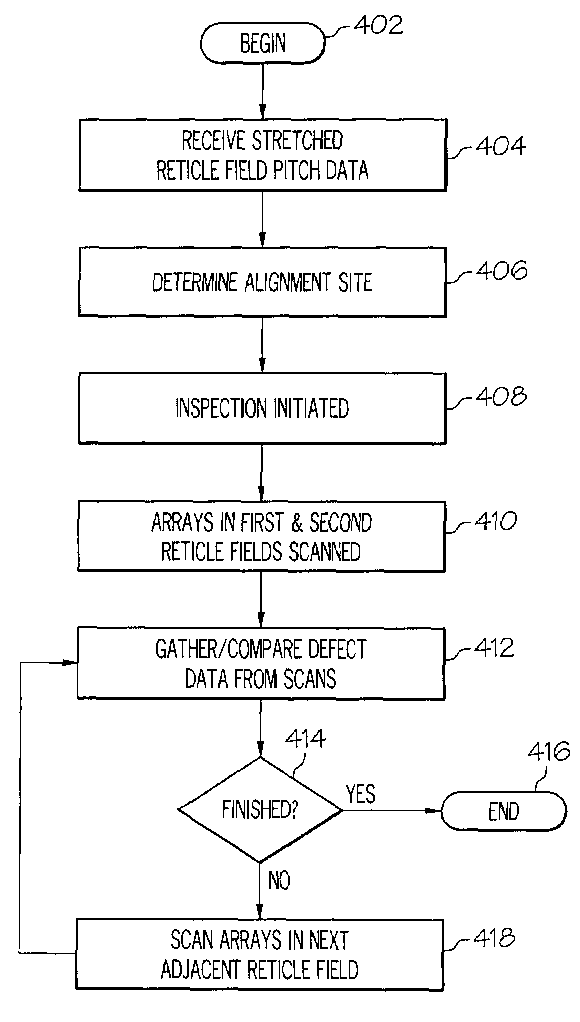
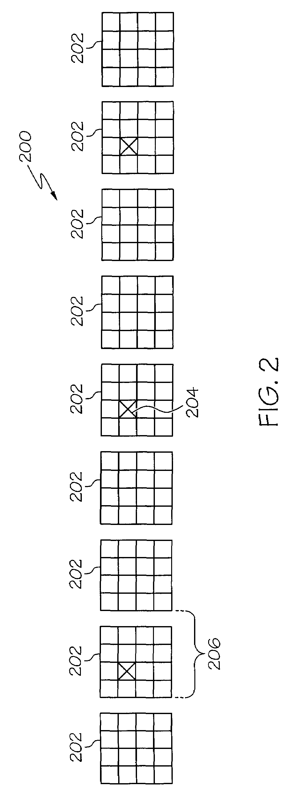
[0020]Exemplary embodiments include a method, apparatus and computer program product for optimizing inspection recipe monitoring activities. The apparatus includes a test structure consisting of a series of arrays, which may resemble circuitry in a product chip, e.g., SRAM. The test structure may be a semiconductor substrate. Each array includes a number of cells. Every third array includes one or more programmed defects. The test structure is then tested using a modified reticle field pitch (referred to herein as “stretched reticle field pitch”) as the new pitch. In one exemplary embodiment, the stretched reticle field pitch is defined as the reticle field pitch plus an inter-array pitch.

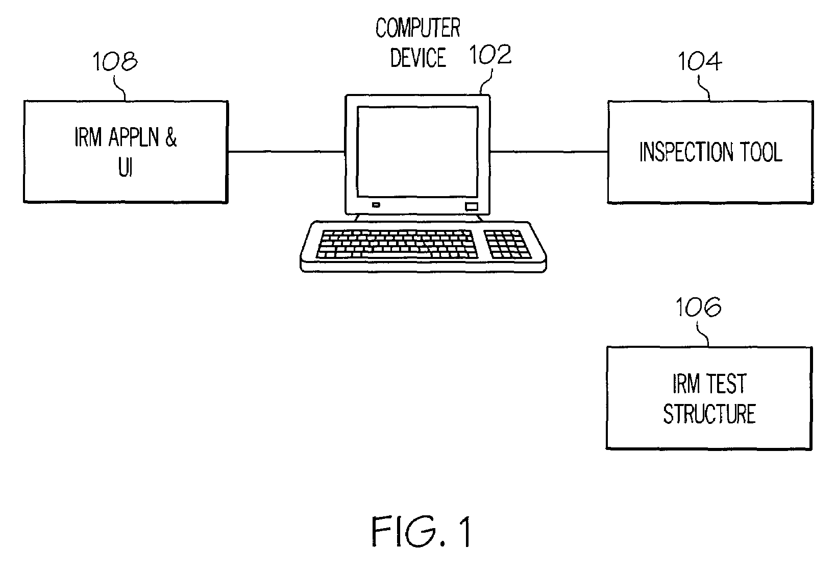
[0021]Turning now to FIG. 1, a system upon which the inspection recipe monitoring activities may be implemented in exemplary embodiments will now be described. The system of FIG. 1 may be part of a manufacturing facility that produces semiconductor products. The system of FIG. 1 includes a computer...


PUM

PropertyMeasurementUnit
distanceaaaaaaaaaa
sizeaaaaaaaaaa
defectaaaaaaaaaa

Abstract

A method, apparatus, and computer program product for implementing inspection recipe services are provided. The apparatus includes a test structure including a semiconductor substrate and a number of arrays disposed on the semiconductor substrate. The arrays are linearly arranged and spaced equidistant. Each of the arrays corresponds to a reticle field and includes a number of cells. The test structure also includes a defect programmed into every third array. The defect is programmed in the same location on each third array. The test structure further includes an alignment site defined on the test structure for providing a point of reference upon inspection. The alignment site, in conjunction with a modified reticle pitch extending the distance of one reticle field plus a portion of an adjacent reticle field, are used to perform a random mode inspection of selected arrays in the test structure.

Description

BACKGROUND OF THE INVENTION[0001]The present disclosure relates to a method, apparatus, and computer program product for optimizing inspection recipes using a mask with programmed defects.[0002]Determining, optimizing, and monitoring the sensitivity of optical, laser-based, electron-beam and other inspection tools are of great importance for state-of-art semiconductor process technologies. The sensitivity is typically defined by the size of the smallest defect that the inspection can detect.[0003]One approach for optimizing the sensitivity of an inspection tool utilizes an arbitrary production wafer. Initially, an inspection threshold is set to a very low level so that lots of noise is picked up as well as all of the detectable defects based upon the current inspection tool settings. The smallest defect detected may or may not be the smallest defect that exists on the wafer. The inspection may then be optimized by iteratively adjusting the inspection conditions so that the signal of...

Claims


Application Information

Patent Timeline
Patent Type & Authority Patents(United States)
IPC IPC(8): G01N21/00G01R31/26
CPCG01N21/93G01N21/956
Inventor PATTERSON, OLIVER D.BRODSKY, MARYJANENAFISI, KOUROSH
Owner GOOGLE LLC
Features
  • R&D
  • Intellectual Property
  • Life Sciences
  • Materials
  • Tech Scout
  • Unparalleled Data Quality
  • Higher Quality Content
  • 60% Fewer Hallucinations
Learn More