Planar electron emitter (PEE)

a technology of electron emitter and electron beam, which is applied in the manufacture of electric discharge tubes/lamps, tubes with screens, discharge tubes luminescnet screens, etc., can solve the problems of unreliable, non-recognizable ballistic electrons in highly resistive semiconductors or insulators, and non-recognizable quasi-ballistic electrons in high resistive materials

Inactive Publication Date: 2008-07-15
VISCOR PETR +3
View PDF31 Cites 17 Cited by
  • Summary
  • Abstract
  • Description
  • Claims
  • Application Information

AI Technical Summary

Benefits of technology

This patent describes how to control which parts of a computer screen get electric current that causes them to glow up. There are different ways this can be done with special materials called luminescers or color TV phosphors. These materials can be placed on top of the screen or another object.

Problems solved by technology

The technical problem addressed in this patent is finding ways to improve the performance of electronic materials in terms of lifetimes, thermal conductivity, and power consumption compared to traditional methods like Cathode Ray Tubes (CRTs) without creating issues related to heat generation, slow downstream manufacturing costs, and lack of reliable design options. This is achieved by introducing a novel method called Planar Electron Emitters based on a unique property known as quasimbal Ballistic Electrons (QBE) that allows for the development of more powerful and versatile semiconductor components and devices.

Method used


Image

  • Planar electron emitter (PEE)
  • Planar electron emitter (PEE)
  • Planar electron emitter (PEE)

Examples


example 1

Field Emission Flat Panel Displays (FE-FPD)

[0209]One of the obvious applications of the present invention is its use in the construction of robust, reliable, large, low power dissipation and cheap Field Emission Flat Panel Displays (FE-FPD).

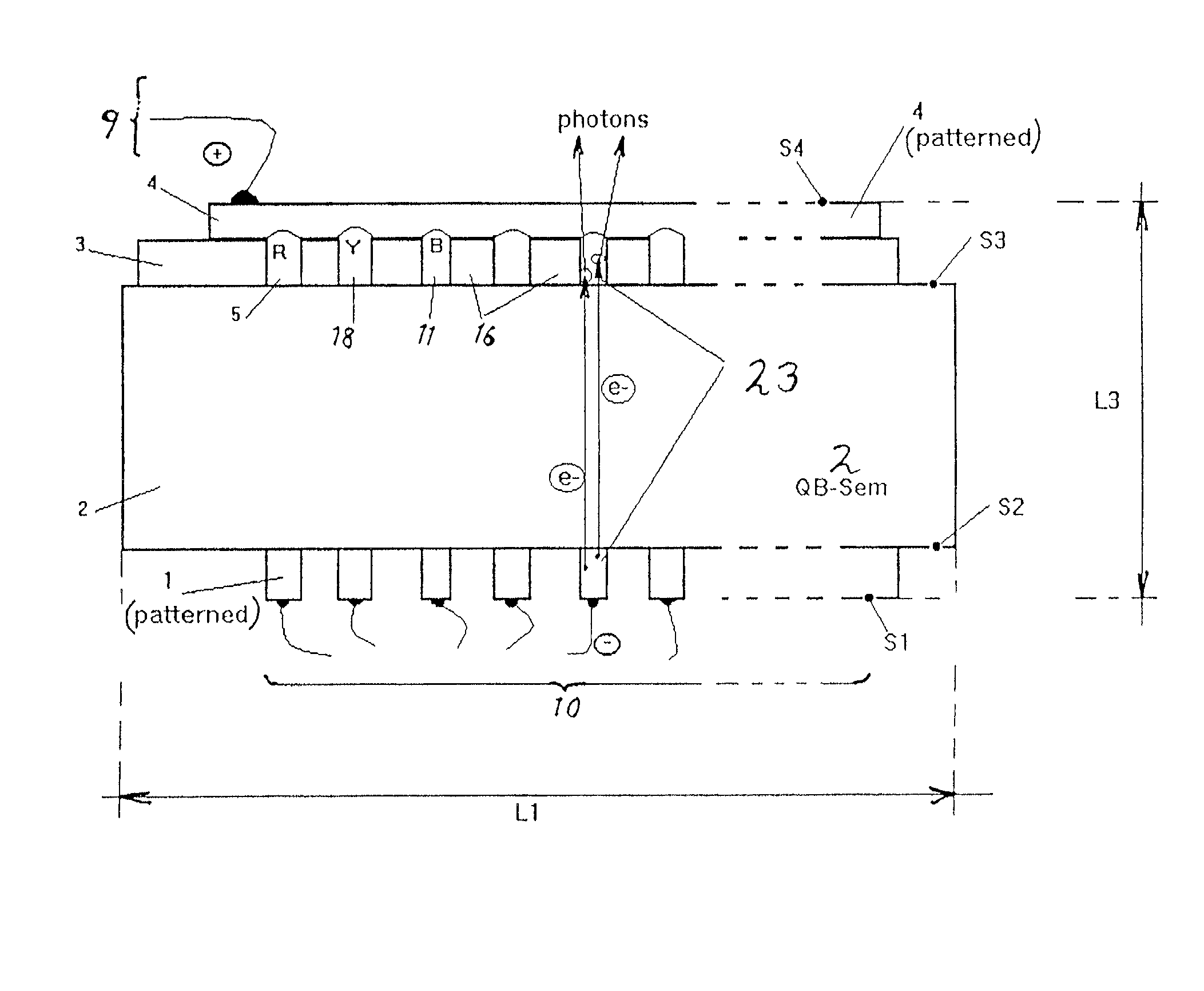
[0210]FIG. 4, which is a cross-sectional diagram along the line A-A of the FE-FPD shown in FIG. 5 is one of the possible vacuum-less FE-FPDs according to the present invention With reference to FIG. 3, the basic planar structure of the present invention—1 (cathode), 2 (QB-Sem) and 4 (anode—optically transparent in this preferred embodiment) is clearly apparent also in FIG. 4. The only difference is that in this Flat Panel Display application of the present invention the cathode and the anode are patterned and that an extra layer 3 is introduced between the surface S3 of the QB-semiconductor and the anode 4. This third layer consists of alternative (patterned) segments of red 5, yellow 18 and blue 11 phosphors or other colour light emitting lumino...

example 2

Planar Electron Beam Lithography

[0219]By using the planar electron emitter according to the present invention the major drawback imposed by the short lifetime of the prior art planar electron emitters, are solved. The present invention offers a qualitatively new and robust solution to the present day needs of the semiconductor industry. The method and the embodiment are described in FIGS. 9 to 14.

[0220]The schematic diagram of the principle behind the Planar Electron Beam Lithography, was described in the prior art using FIG. 8. In the prior art, an electron lithographic projection system has been demonstrated using a prior art planar electron emitter. The planar electron emitter of the present invention can be directly implemented in place of the prior art emitter.

[0221]One possible embodiment according to the present invention of such a planar electron emitter structure is shown in FIG. 10. The major difference from prior art FIG. 8 is the replacement of a thin film oxide layer 24...

example 3

Two-Dimensional Illumination Panels

[0226]Due to the simplicity of design, robustness, low power dissipation, low temperature operation and two-dimensional nature of the planar electron emitter according to the present invention, the said planar electron emitter can be used very conveniently in the construction of two-dimensional (planar and non-planar) illumination sources.

[0227]One such possible flat illumination panel is shown schematically in FIGS. 15 and 16. Here the basic structure of the planar electron emitter (cathode 1, QB-semiconductor 2 and the anode 4) is used as planar source of electrons (when an appropriate electrical voltage is applied between the cathode and the anode) emerging into the free space FS. These electrons are accelerated within this space by means of the accelerating electrode 7 and enter the light emitting layer 3. The optically transparent plate 13 (typically a glass plate) that allows the generated light to escape from the said structure forms (togeth...


PUM


Abstract

A planar electron emitter, based on the existence of quasi-ballistic transport of electrons is disclosed. In its preferred embodiment the planar electron emitter structure consists of a body of finite gap pure semiconductor or insulator, the said body of macroscopic thickness (˜1 mm) being terminated by two parallel surfaces and of a set of two electrodes deposited/grown on the said two free surfaces such that when a low external electrical field (˜100 V/cm) is applied to this structure, consisting of two electrodes and the said semiconductor or insulating body sandwiched between them, a large fraction of electrons injected into the said semiconductor or insulator body from the negatively charged electrode (cathode) is quasi-ballistic in nature, that is this fraction of injected electrons is accelerated within the said semiconductor or insulator body without suffering any appreciable inelastic energy losses, thereby achieving sufficient energy and appropriate momentum at the positively charged electrode (anode) to be able to traverse through the said anode and to escape from the said structure into empty space (vacuum), said semiconductor or insulator body comprises a material or material system having a predetermined crystal orientation.

Description


Claims


Application Information

Patent Timeline
Owner VISCOR PETR
Why Eureka
Try Eureka