Semiconductor chip package with a package substrate and a lid cover
- Summary
- Abstract
- Description
- Claims
- Application Information
AI Technical Summary
Benefits of technology
Problems solved by technology
Method used
Image

Examples
Embodiment Construction
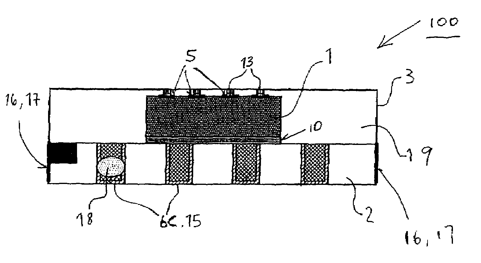
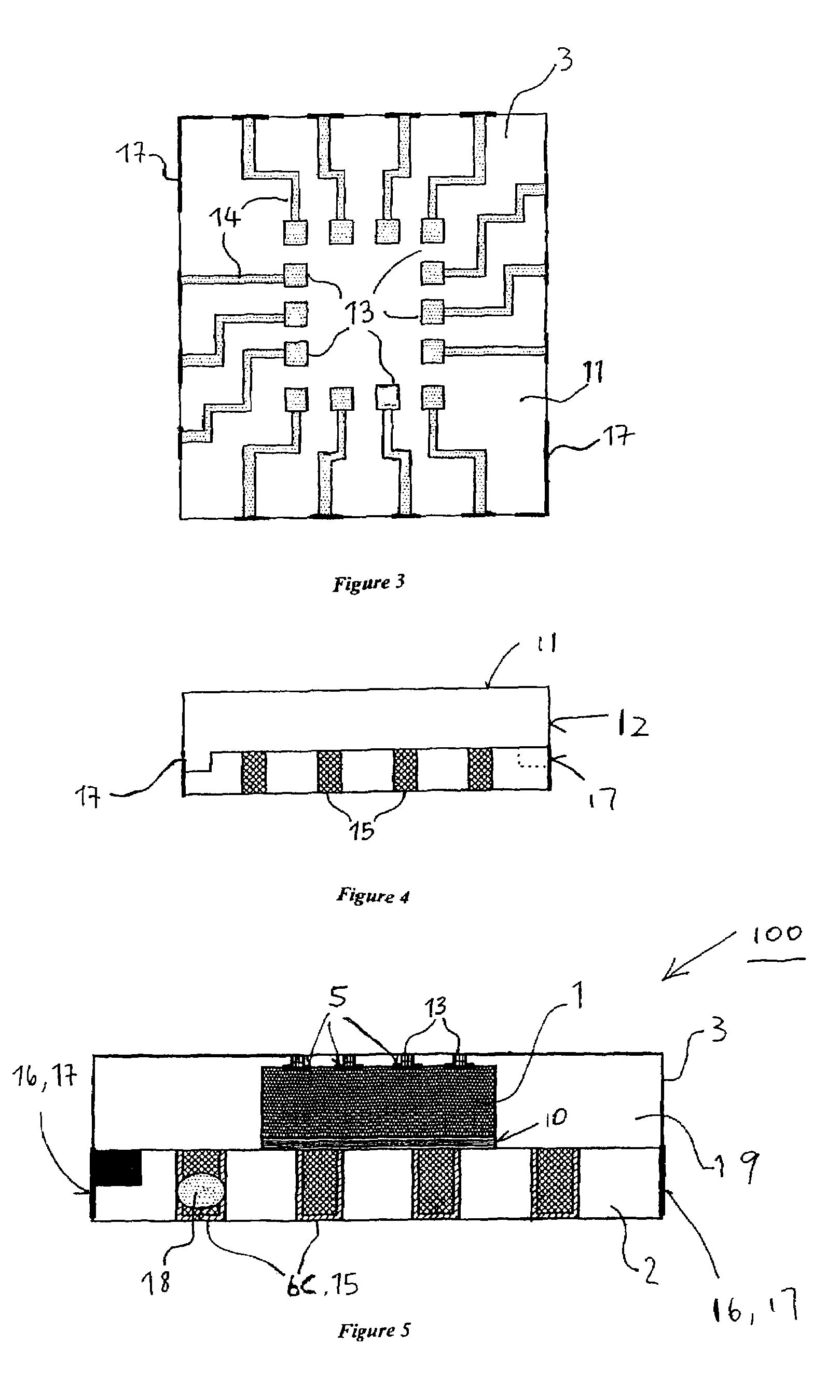
[0017]FIG. 5 shows a side view of a semiconductor chip package 100 in accordance with one embodiment of the present invention. As will be described in more detail below, the semiconductor chip package 100 is a wireless semiconductor chip package. This means that the package 100 is without connecting and self-supported wires. The semiconductor chip 1 can also be referred to as a semiconductor (or IC) chip or die.
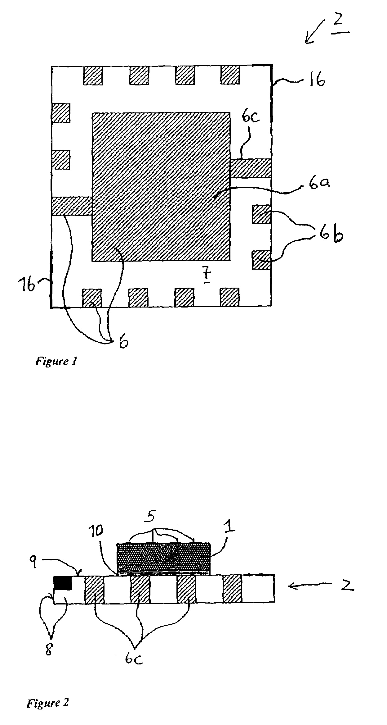
[0018]The semiconductor chip package 100 includes a semiconductor chip 1. The semiconductor chip 1 has a top bond pad pattern 5. The semiconductor chip 1 is housed between a package substrate 2 and a lid cover 3. The lid cover 3 is fitted onto the package substrate 2. The lid cover 3 is internally plated with a bottom bond pad pattern 13 corresponding to and in contact with the top bond pad pattern 5 of the semiconductor chip 1 and provides internal conductor traces to electrically connect the semiconductor chip 1 to a bottom bond pad pattern 6 of the package substrate 2.
[001...
PUM
 Abstract
Description
Claims
Application Information