Metal coated nanocrystalline silicon as an active surface enhanced raman spectroscopy (SERS) substrate

a technology of active surface and substrate, applied in the field of metal-coated porous substrate, can solve the problems of limited applicability of raman analysis, low sensitivity and limited raman spectroscopy performance, and low enhancement factor

Inactive Publication Date: 2008-07-15
INTEL CORP
View PDF18 Cites 24 Cited by
  • Summary
  • Abstract
  • Description
  • Claims
  • Application Information

AI Technical Summary

Problems solved by technology

The probability of Raman interaction occurring between an excitatory light beam and an individual molecule in a sample is very low, resulting in a low sensitivity and limited applicability of Raman analysis.
However, the number of metal particles that can be deposited on a planar surface is limited, producing a relatively low enhancement factor for SERS and related Raman techniques utilizing such surfaces.

Method used


Image

  • Metal coated nanocrystalline silicon as an active surface enhanced raman spectroscopy (SERS) substrate
  • Metal coated nanocrystalline silicon as an active surface enhanced raman spectroscopy (SERS) substrate
  • Metal coated nanocrystalline silicon as an active surface enhanced raman spectroscopy (SERS) substrate

Examples


example 1

Construction of a Raman Active Substrate

Formation of Porous Nanocrystalline Silicon

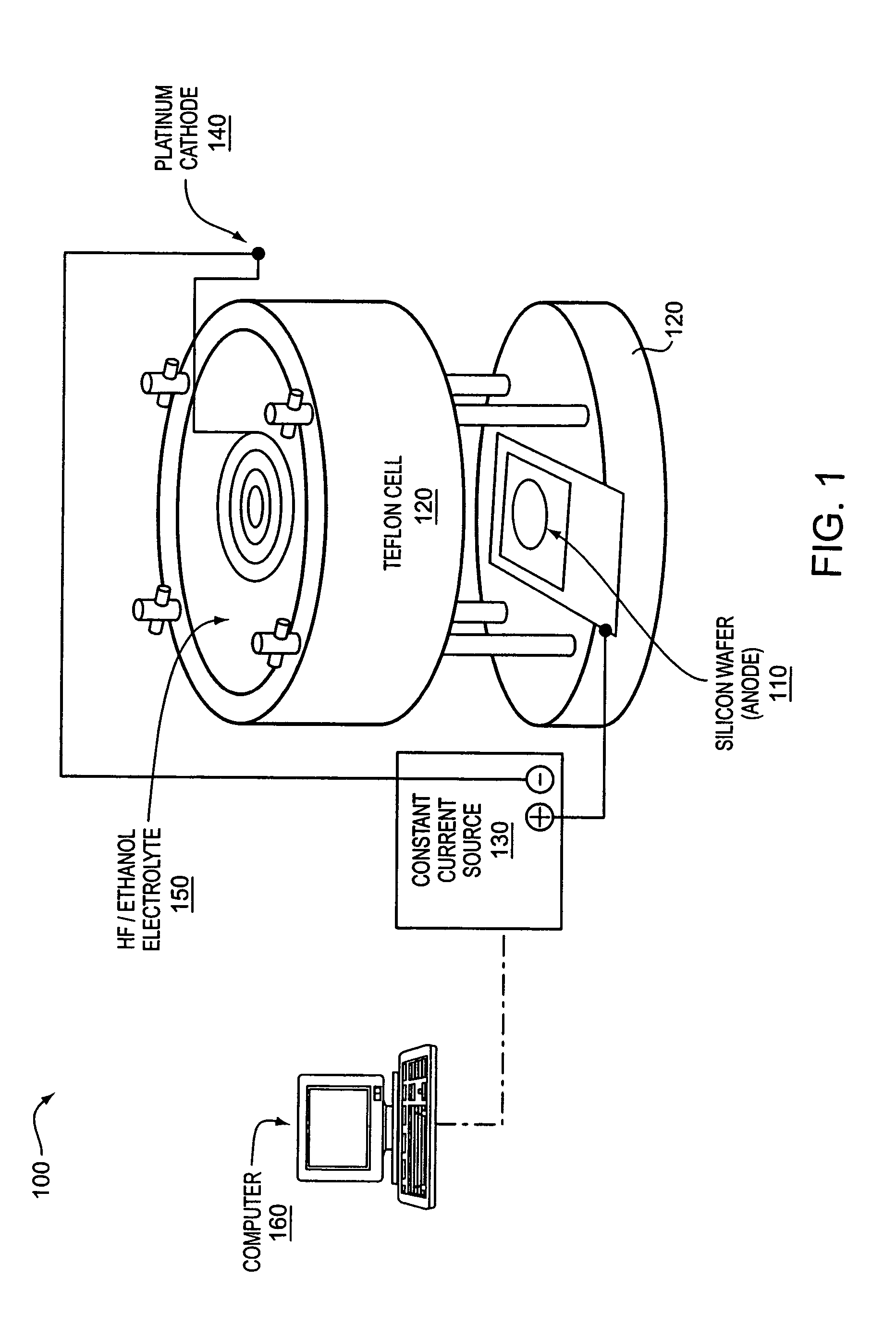
[0069]An exemplary method and apparatus 100 for forming nanocrystalline porous silicon substrates 110 is illustrated in FIG. 1. Methods for making nanocrystalline porous silicon are known in the art (e.g., U.S. Pat. No. 6,017,773). A layer of nanocrystalline porous silicon may be formed electrochemically as disclosed in Petrova-Koch et al. (Appl. Phys. Let. 61:943, 1992). Depending on the particular application, the silicon may be lightly or heavily p-doped or n-doped prior to etching to regulate the characteristics of the porous silicon substrate 110. Single crystal silicon ingots may be fabricated by the well known Czochralski method (e.g., http: / / www.msil.ab.psiweb.com / english / msilhist4-e.html). A single crystal silicon wafer 110 may be treated with anodic etching in dilute HF / ethanol 150 to form a nanocrystalline porous silicon substrate 110. Alternatively, chemical etching in a solution of HF, ni...

example 2

Metal Coating of Porous Silicon by Thermal Decomposition

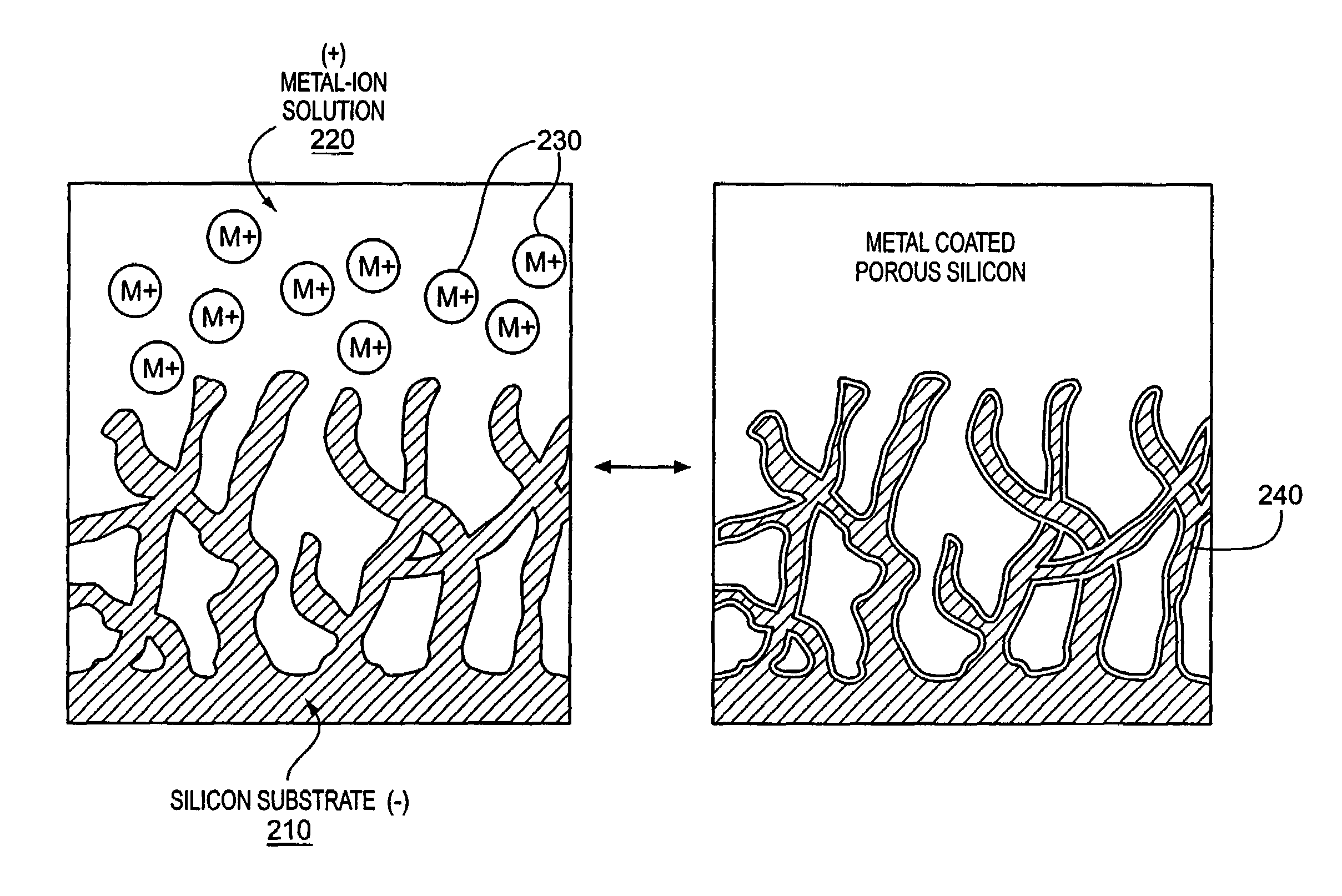
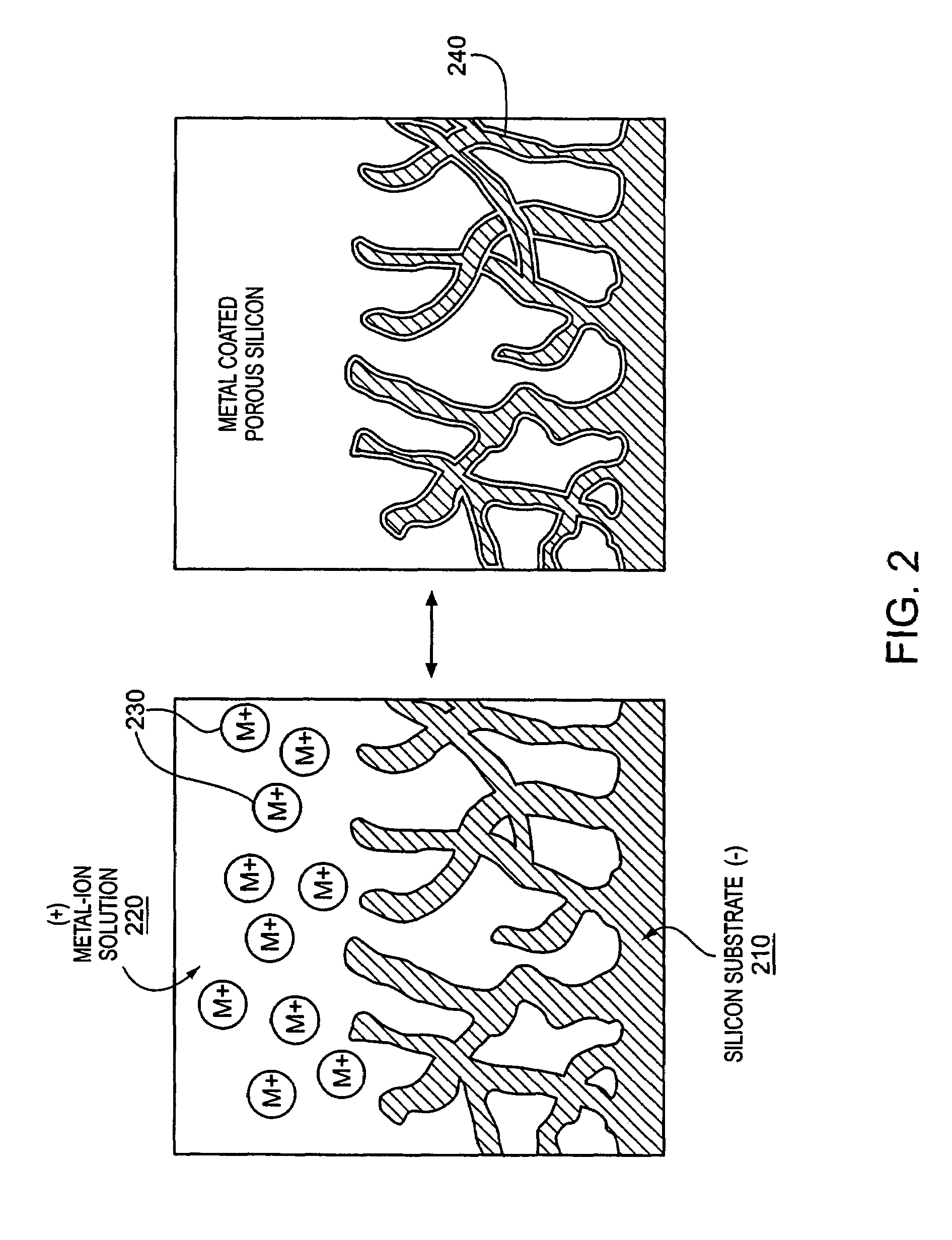
[0074]FIG. 4 illustrates an exemplary method for uniformly impregnating metal 450 into nanoporous silicon. The surface of the porous silicon is oxidized to silicon dioxide (FIG. 4B). A metal salt solution is diffused into the porous matrix (FIG. 4C) and dried (FIG. 4E). The dried metal salt is thermally decomposed inside the pores to form a uniform metal layer (FIG. 4F). Oxidation of the porous silicon surface enables complete wetting of porous silicon in the metal salt solution, while preventing spontaneous immersion coating, which causes pore blockage. The dry metal salt is thermally decomposed in a furnace and pure metal is deposited on the side walls of the nanopores. A uniform, thin metal coating of nanoporous silicon may be obtained without plugging the pores, as often observed with standard methods of metal infiltration into nanoporous silicon. Currently available plating methods are also diffusion limited, resulting in ...

example 3

Raman Detection of Analytes

[0080]As exemplified in FIG. 3, a Raman active metal-coated substrate 340 formed as disclosed above may be incorporated into an apparatus 300 for Raman detection, identification and / or quantification of analytes. The substrate 340 may be incorporated into, for example, a flow through cell 330, connected to inlet 320 and outlet 350 channels. The inlet channel 320 may be connected to one or more other devices 310, such as a sample injector 310 and / or reaction chamber 310. Analytes may enter the flow through cell 330 and pass across the Raman active substrate 340, where they may be detected by a Raman detection unit 360. The detection unit 360 may comprise a Raman detector 380 and a light source 370, such as a laser 370. The laser 370 may emit an excitation beam 390, activating the analytes and resulting in emission of Raman signals. The Raman signals are detected by the detector 380. In certain embodiments of the invention, the detector 380 may be operably c...


PUM

PropertyMeasurementUnit
pore sizeaaaaaaaaaa
porositiesaaaaaaaaaa

Abstract

The disclosed methods and apparatus concern Raman spectroscopy using metal coated nanocrystalline porous silicon substrates. Porous silicon substrates may be formed by anodic etching in dilute hydrofluoric acid. A thin coating of a Raman active metal, such as gold or silver, may be coated onto the porous silicon by cathodic electromigration or any known technique. In certain alternatives, the metal coated porous silicon substrate comprises a plasma-oxidized, dip and decomposed porous silicon substrate. The metal-coated substrate provides an extensive, metal rich environment for SERS, SERRS, hyper-Raman and / or CARS Raman spectroscopy. In certain alternatives, metal nanoparticles may be added to the metal-coated substrate to further enhance the Raman signals. Raman spectroscopy may be used to detect, identify and / or quantify a wide variety of analytes, using the disclosed methods and apparatus. In some disclosed methods, Raman spectroscopy may be used to detect nucleotides, purines or pyrimidines at the single molecule level.

Description

RELATED APPLICATIONSCROSS REFERENCE TO RELATED APPLICATIONS[0001]This application is a continuation application of U.S. application Ser. No. 10 / 680,583 filed Oct. 7, 2003, now U.S. Pat. No. 6,989,897; which is a continuation-in-part application of U.S. application Ser. No. 10 / 368,976 filed Feb. 18, 2003, now pending; which is a continuation-in-part application of U.S. application Ser. No. 10 / 171,357 filed Jun. 12, 2002, now U.S. Pat. No. 6,970,239. The disclosure of each of the prior applications is considered part of and is incorporated by reference in the disclosure of this application.FIELD OF THE INVENTION[0002]The present methods and apparatus relate to the fields of molecular detection and / or characterization by Raman spectroscopy. More particularly, the methods and apparatus concern metal-coated porous substrates for surface enhanced Raman spectroscopy (SERS), surface enhanced resonance Raman spectroscopy (SERRS), hyper-Raman and / or coherent anti-Stokes Raman spectroscopy (CA...

Claims


Application Information

Patent Timeline
Patent Type & Authority Patents(United States)
IPC IPC(8): G01J3/44C12Q1/68G01N21/65
CPCC12Q1/6825G01J3/44G01N21/658B82Y15/00B82Y30/00G01N2021/6439G01N2021/656G01N2021/655G01N2021/653C12Q2565/632C12Q2563/155
Inventor CHAN, SELENABERLIN, ANDREW A.KWON, SUNGHOONSUNDARARAJAN, NARAYANANYAMAKAWA, MINEO
Owner INTEL CORP
Why Eureka
Try Eureka