Quick high-flexibility manufacturing method for ceramic circuit board

A circuit board, fast technology, applied in the direction of printed circuit manufacturing, printed circuits, manufacturing tools, etc., can solve the problems of many processes, poor precision, low flexibility, etc.

Active Publication Date: 2013-07-03
SHENZHEN SUNSHINE LASER & ELECTRONICS TECH CO LTD
View PDF3 Cites 47 Cited by
  • Summary
  • Abstract
  • Description
  • Claims
  • Application Information

AI Technical Summary

Problems solved by technology

[0007] The purpose of the present invention is to provide a method for fast and highly flexible production of ceramic circuit boards, to produce high-precision and high-density ceramic circuit boards, and to solve the shortcomings of the traditional ceramic circuit board production process, such as many procedures, long process, poor precision, and low flexibility.

Method used


Image

  • Quick high-flexibility manufacturing method for ceramic circuit board
  • Quick high-flexibility manufacturing method for ceramic circuit board
  • Quick high-flexibility manufacturing method for ceramic circuit board

Examples


example 1

[0030] 1) The ceramic material is made of 99% high-purity aluminum nitride ceramics, which are made into ceramic substrates by tape casting. The thickness is 0.1-2mm, the surface roughness Ra is 0.3-0.5μm, and the roughness can reach 0.03μm after polishing.

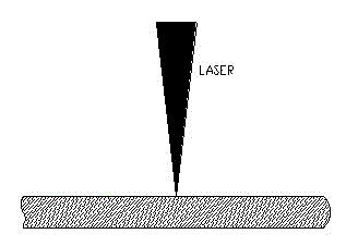
[0031] 2) Use ultraviolet 355nm nanosecond pulsed laser to drill and modify high-purity aluminum nitride ceramics. The laser source adopts ultraviolet 355nm nanosecond pulse laser, the maximum average laser output power is 10W, the pulse width is 1-10ns, and the pulse repetition frequency is 1-400kHz.

[0032] Laser drilling is preferably carried out with high power, high pulse repetition frequency, and high scanning speed. For example, if the average laser output power is 10W, the pulse repetition frequency is 100kHz, and the scanning speed is 100mm / s, fast drilling can be achieved, and the hole wall can also be laser modified. sex.

[0033] During laser surface modification, the energy density is controlled above the m...

example 2

[0038] 1) The ceramic material is 96% alumina ceramic, which is made into a three-dimensional ceramic matrix by casting method, and the surface roughness Ra is 0.3-0.5μm.

[0039]2) A picosecond pulsed laser with a center wavelength of 266nm is used to drill holes and modify the surface of alumina ceramics. The laser source adopts a picosecond pulse laser with a central wavelength of 266nm, the maximum average laser output power is 5W, the pulse width is 1-10ps, and the pulse repetition frequency is 100kHz-1MHz.

[0040] For laser drilling, when the average laser output power is 5W, the pulse repetition frequency is 1MHz, and the scanning speed is 50mm / s, the drilling is carried out in a focusing manner, and the focusing height decreases with the drilling depth, and multiple scans are performed until the drilling through or to the desired depth of the blind hole. Picosecond laser is an ultrashort pulse laser with short pulse width and high peak energy, which has great advanta...


PUM

PropertyMeasurementUnit
thicknessaaaaaaaaaa
thicknessaaaaaaaaaa
thicknessaaaaaaaaaa

Abstract

A quick high-flexibility manufacturing method for a ceramic circuit board comprises the following steps: irradiating laser on the surface of a ceramic matrix, and controlling the energy density of the laser to reach above the fracture threshold of the chemical bond of the compound containing active ions, so that chemical reaction occurs on the surface of the ceramic matrix, an active substance is separated out to serve as a chemical plating catalytic source, and the active substrate generated by the reaction and the matrix form chemical metallurgical bonding, wherein different laser sources are selected aiming at different ceramic materials according to the chemical bond energy of the ceramic material components, and the laser energy is controlled to reach the ceramic modified threshold by controlling the average power of laser output, pulse repetition frequency, scanning speed, defocusing amount, space between scanning line and scanning times; and the ceramic matrix modified by the laser is placed into a chemical plating solution to perform plating to form a metal coating. The surface of the ceramic is modified by the laser, so that a metal conductive layer and the matrix form chemical metallurgical bonding, the bonding force of the circuit board is greatly increased, and the heat-conducting property and the electric property are improved.

Description

technical field [0001] The invention relates to the field of circuit board production, in particular to a method for fast and highly flexible production of ceramic circuit boards. Background technique [0002] With the rapid development of electronic technology towards high integration and miniaturization, the wires and electronic components of circuit boards are becoming more and more dense, and the problem of heat dissipation is becoming more and more prominent. Ceramic materials have high thermal conductivity and good electrical properties. They are ideal heat dissipation and packaging materials for a new generation of large-scale integrated circuits, semiconductor module circuits and high-power devices. Therefore, ceramic circuit boards have received widespread attention and rapid development. Compared with traditional printed circuit boards, ceramic circuit boards obviously have many advantages: excellent thermal conductivity, chemical corrosion resistance, large insula...

Claims


Application Information

Patent Timeline
Patent Type & Authority Applications(China)
IPC IPC(8): H05K3/00H05K3/18B23K26/00B23K26/38B23K26/382
Inventor 蔡志祥文明侯若洪
Owner SHENZHEN SUNSHINE LASER & ELECTRONICS TECH CO LTD
Why Eureka
Try Eureka