

Display device, driving method thereof, and electronic apparatus
- Summary
- Abstract
- Description
- Claims
- Application Information
AI Technical Summary
Benefits of technology
Problems solved by technology
Method used
Image

Examples
embodiment mode 1
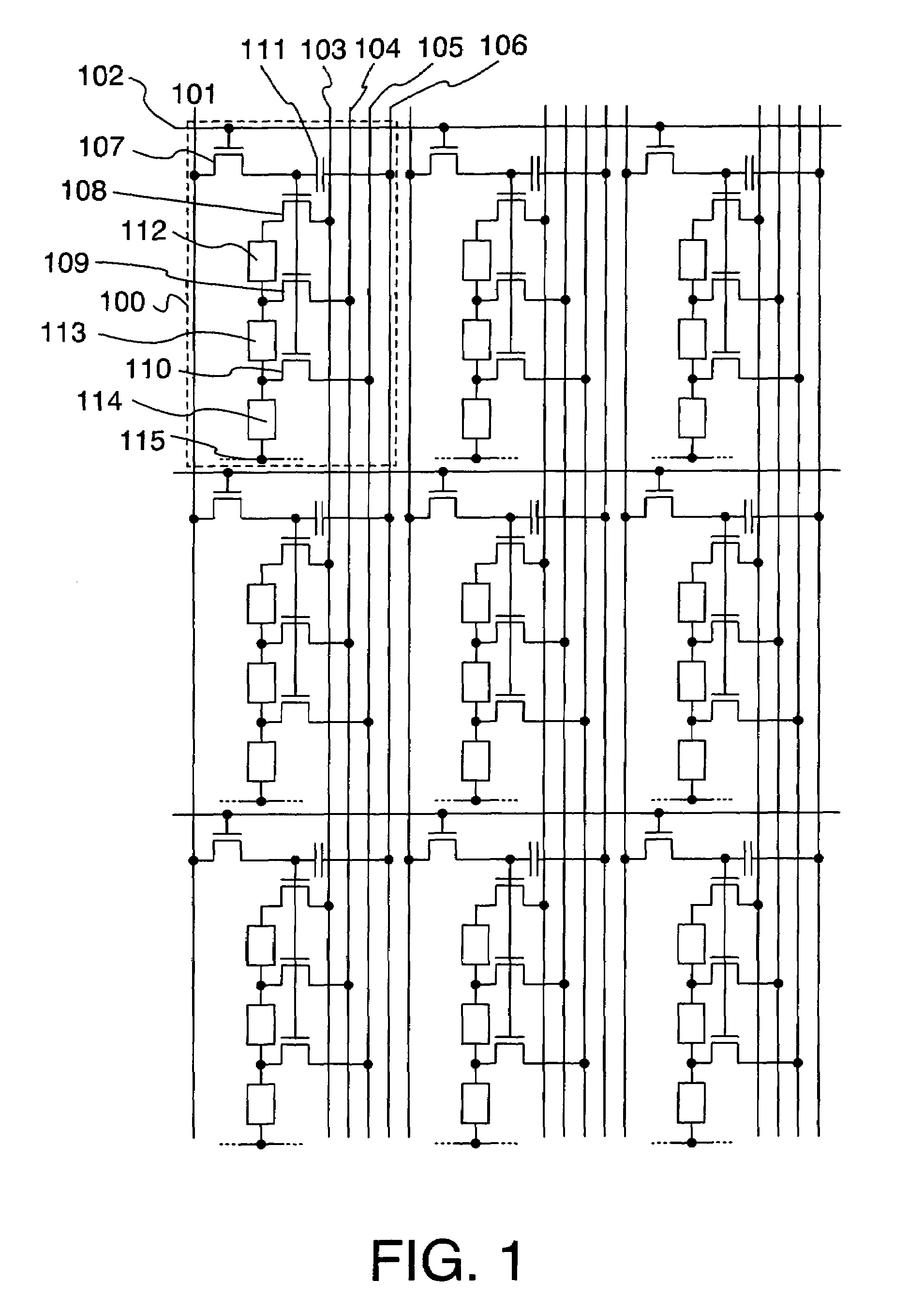
[0042]FIG. 1 shows the configuration of a pixel portion in a display device of the present invention. Although the present invention will be described hereinafter while using, as an example of a transistor, a thin film transistor (referred to below as a “TFT”) formed on an insulator, the present invention is not limited thereto and includes all cases where the transistor is configured by using an organic thin film transistor, a MOS transistor, a molecular transistor or the like. Also, because it is difficult to separate the source region and the drain region in a TFT due to the configuration and operating conditions thereof, one will be referred to as a first electrode and the other will be referred to as a second electrode. Although the present invention will be described using EL elements as an example of light-emitting elements, the present invention is not limited thereto and includes, as targets, elements with which an electrical current can be generated by imparting a potentia...
embodiment mode 2
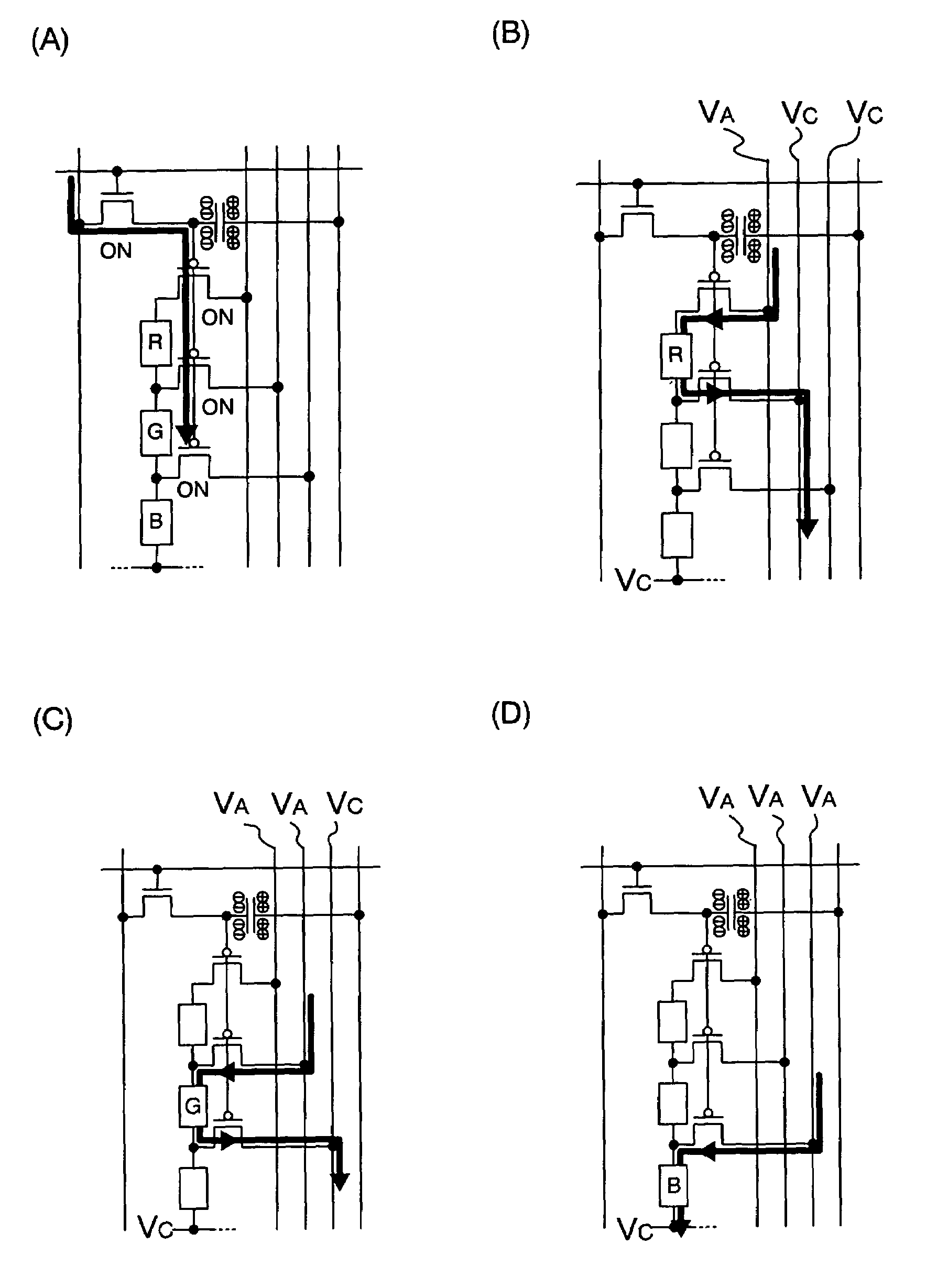
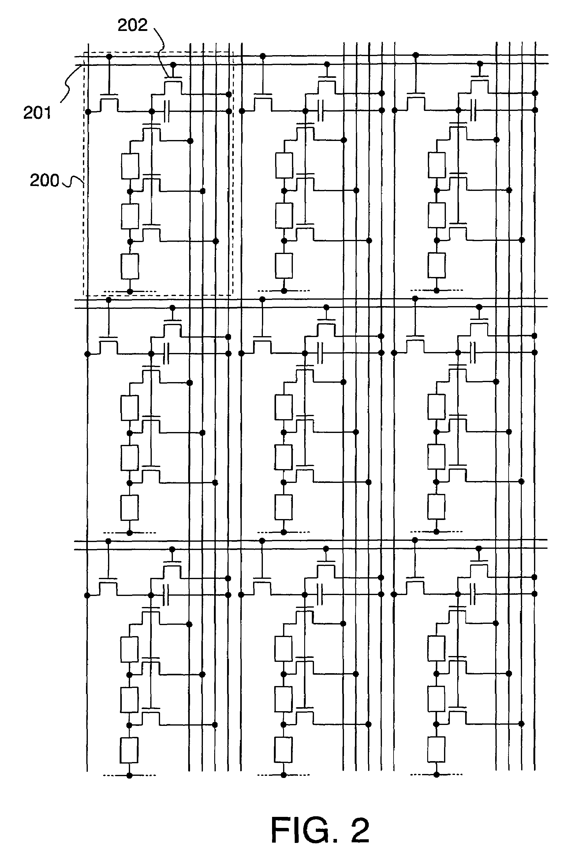
[0060]FIG. 2 shows an example where the present invention is applied to pixels of a configuration that is different from those of embodiment mode 1. A gate signal line for erasure 201 and a TFT for erasure 202 are added to the configuration shown in FIG. 1. Because the remaining configuration is in accordance with FIG. 1, numbers will be omitted.
[0061]With respect to the pixels of the configuration shown in FIG. 2, the EL elements emitting light can be forcibly placed in a non-light-emitting state at a desired timing in order to control the emission time when conducting display according to the digital time gradation described in Japanese Patent Laid-open No. 2001-343933. Specifically, a line selection pulse is outputted to the gate signal line for erasure 201 at the timing at which one desires to end light emission, whereby the TFT for erasure 202 is turned ON. Thus, the potentials of the gate electrodes of the TFTs for driving 108 to 110 become equal to the potential of the retent...
embodiment
Embodiment 1
[0065]In the present embodiment, the configuration of a drive circuit for controlling pixels configured by using the present invention will be described.
[0066]FIG. 6 shows a configuration example of a source signal line drive circuit for conducting display using analog image signals as mainly image signals.
[0067]In the example of FIG. 6(A), the source signal line drive circuit includes a shift register 602 using a plurality of flip-flops 601, NANDs 603, level shifters 604, buffers 605 and sampling switches 606.
[0068]The operation will be described. The shift register 602 sequentially outputs sampling pulses in accordance with clock signals (S-CK, S-CKb) and a start pulse (S-SP). Sometimes two continuous sampling pulses have a period in which their mutual pulses overlap. In such a case, computation is conducted with the before and after sampling pulses by the NANDs 603. Depending on the configuration of the shift register 602, sometimes the NANDs 603 are not necessary.
[00...
PUM
 Abstract
Description
Claims
Application Information