
Method for detecting bisection pattern in deinterlacing

a bisection pattern and deinterlacing technology, applied in the field of image processing, can solve the problems of misdetecting of conventional edge direction detection techniques, and achieve the effect of improving the detection capability of low angle direction

Active Publication Date: 2008-07-22
SAMSUNG ELECTRONICS CO LTD
View PDF5 Cites 11 Cited by
  • Summary
  • Abstract
  • Description
  • Claims
  • Application Information

AI Technical Summary

Benefits of technology

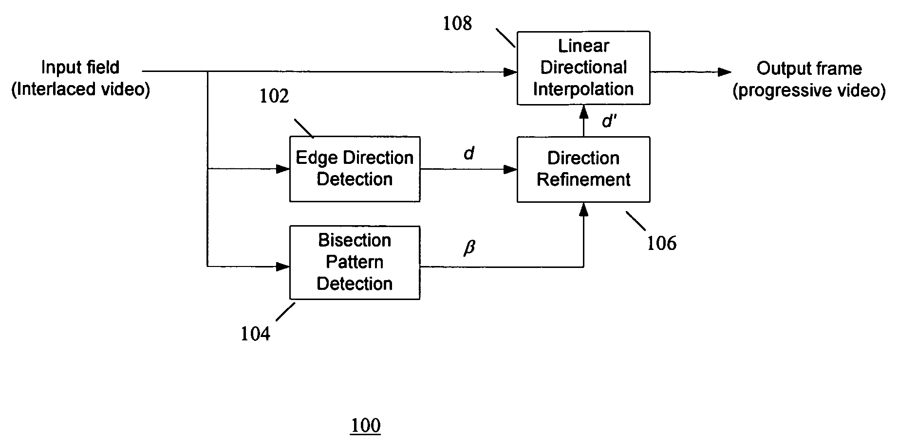
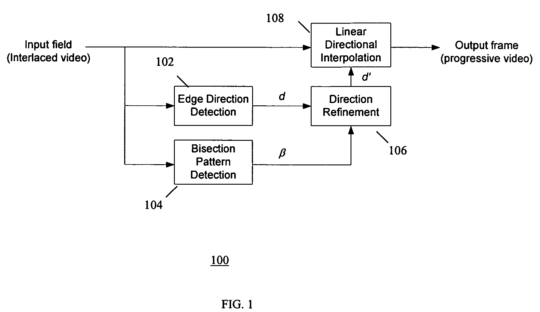
The present invention provides a method for improving low angle direction detection capability in interlaced videos. This is achieved by detecting a Bisection pattern and using it in conjunction with deinterlacing. The method involves constructing a window around each missing pixel in the video and generating a binary map based on the values in the window. The number of value changes in the map is then counted to determine if the missing pixel is within the Bisection pattern. Deinterlacing is then performed to improve the video quality. The method can identify complicated areas and maintain both low angle edge direction detection capability and low misdetection probability. The technical effect of the invention is to enhance the detection of low angle direction in interlaced videos.

Problems solved by technology

In deinterlacing, conventional edge direction detection techniques typically misdetect when direction |d| is large (the very low angle direction).

Method used


Image

  • Method for detecting bisection pattern in deinterlacing
  • Method for detecting bisection pattern in deinterlacing
  • Method for detecting bisection pattern in deinterlacing

Examples


Embodiment Construction

[0016]In one embodiment, the present invention applies Bisection pattern detection in conjunction with deinterlacing. The general idea of the Bisection pattern is briefly discussed while its strict definition will be later delineated mathematically in the detailed description of the preferred embodiment section. Conceptually, the pattern of a collection of pixels within some window (or area) is called Bisection pattern if those pixels can be clearly separated into two regions (or sections): (1) a region containing pixels whose gray levels are greater than a sample mean in that area, and (2) a region containing pixels whose gray levels are not greater than a sample mean in that area. The areas containing Bisection patterns are very well-structured areas and are considered uncomplicated areas. An example of the Bisection pattern within a specified window is shown in FIG. 4. In FIG. 4, an example of the Bisection pattern within a window W is provided. FIG. 4 shows a portion of field 40...


PUM


Abstract

A method for detecting the Bisection pattern for use in conjunction with the deinterlacing is to improve low angle direction detection capability. A method of Bisection pattern detection operates in an interlaced video containing both top and bottom fields. For each missing pixel in a current input field, a window W is constructed whose center pixel is at the considered missing pixel. A binary map is generated which includes rows of values corresponding to pixels in the window, wherein the values indicate if each element of the window is greater than the sample mean of the area surrounding the missing pixel. The number of value changes in the values in each row of the binary map is counted. It is then determined whether or not the missing pixel is within the Bisection pattern based on said counts. In order to maintain both the low angle edge direction detection capability and low misdetection probability, complicated areas are identified by the Bisection pattern detection method. Then deinterlacing is performed.

Description

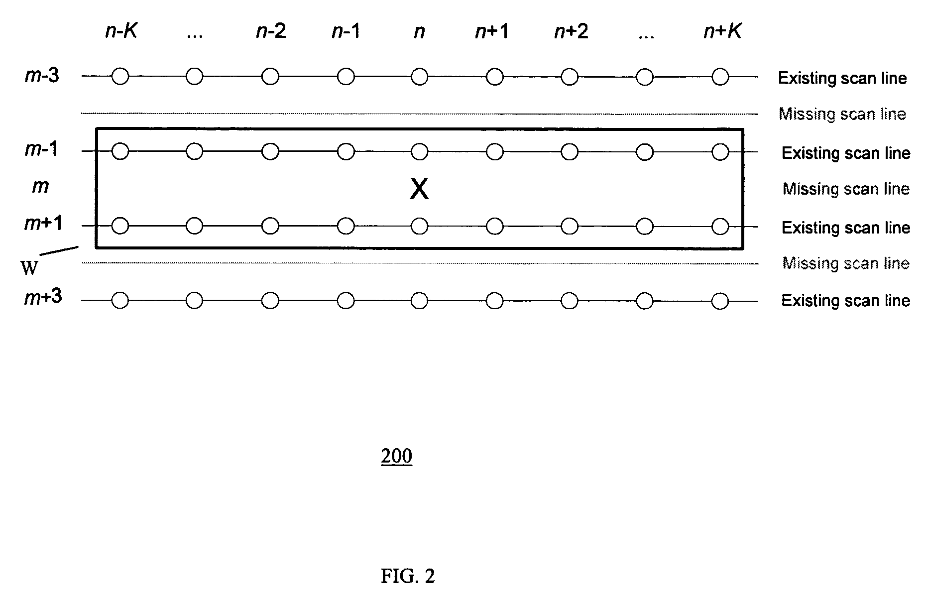
FIELD OF THE INVENTION[0001]The present invention relates to the field of image processing, and more particularly, to the application of Bisection detection algorithm in conjunction with edge direction detection for video deinterlacing in order to improve the misdetection probability of the low angle direction.BACKGROUND OF THE INVENTION[0002]Due to the recent advances of digital television (DTV), deinterlacing plays an important role in standard conversion between interlaced and progressive video scanning formats. For an image display of size M×N, where M and N denote the number of scan lines and number of pixels in each scan line, respectively, in an interlaced video scanning format, the picture formed by the stack of all even scan line m=0, 2, 4, . . . , M−2 is called top field (or even field). Each even scan line of the top field is called existing scan line while its odd counterpart whose pixels do not exist is called missing scan line. In a similar fashion, the bottom field (o...

Claims


Application Information

Patent Timeline
Patent Type & Authority Patents(United States)
IPC IPC(8): H04N7/01H04N11/20
CPCH04N19/172H04N19/14H04N19/112H04N7/01
Inventor LERTRATTANAPANICH, SURAPONGKIM, YEONG-TAEG
Owner SAMSUNG ELECTRONICS CO LTD
Learn More