Basic cell architecture for structured application-specific integrated circuits

a cell-based integrated circuit and integrated circuit technology, applied in the field of integrated circuits, can solve the problems of low cost, low layout efficiency, and low cost, and achieve the effect of reducing the number of recurring expenses, avoiding recurring costs, and avoiding recurring costs

Inactive Publication Date: 2008-07-22
AVAGO TECH INT SALES PTE LTD
View PDF5 Cites 126 Cited by
  • Summary
  • Abstract
  • Description
  • Claims
  • Application Information

AI Technical Summary

Benefits of technology

[0012]In yet another embodiment, the circuit architecture includes an arrangement of transistors comprising a first pair of gate lines spanning above an n-type diffusion region and two distinct p-type diffusion regions, wherein a width of one of the two p-type diffusion regions is smaller than a width of the other of the two p-type diffusion regions. The circuit architecture further includes a second pair of gate lines dividedly arranged in parallel and on opposing sides of the first pair of gate lines, ...

Problems solved by technology

Often, however, a tradeoff between performance and cost exists for layout considerations.
That is, layout is performed on a chip-by-chip basis and cannot be easily modified whenever a design change is needed for that particular product.
An ASIC thereby enjoys the benefits of high performance, but also has a fairly high non-recurring recurring expense each time a design change is needed.
FPGAs unfortunately have lower performance and higher power consumption relative to ASIC designs.
However, structured ASICs are not programmed in the field as in FPGA...

Method used


Image

  • Basic cell architecture for structured application-specific integrated circuits
  • Basic cell architecture for structured application-specific integrated circuits
  • Basic cell architecture for structured application-specific integrated circuits

Examples


Embodiment Construction

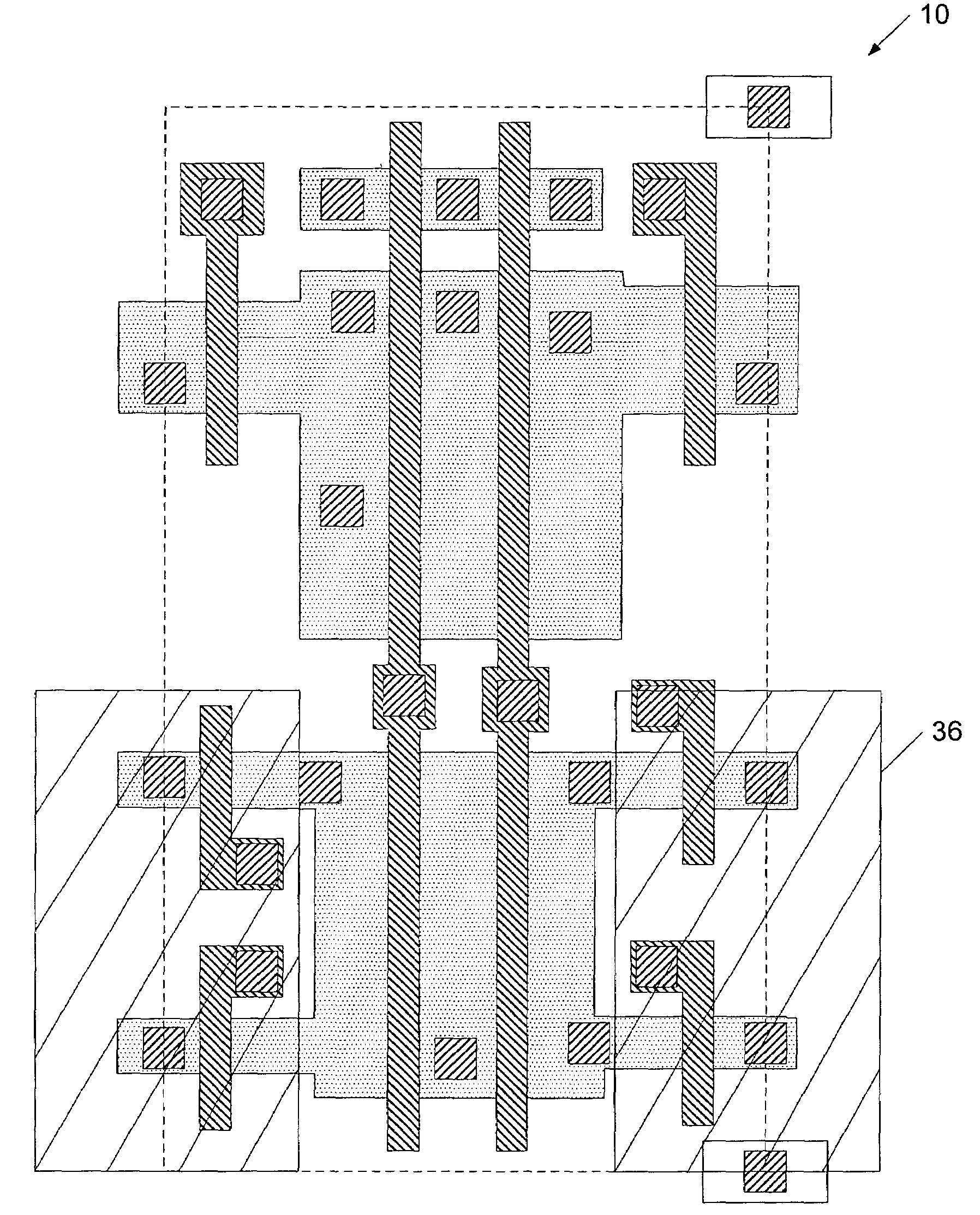
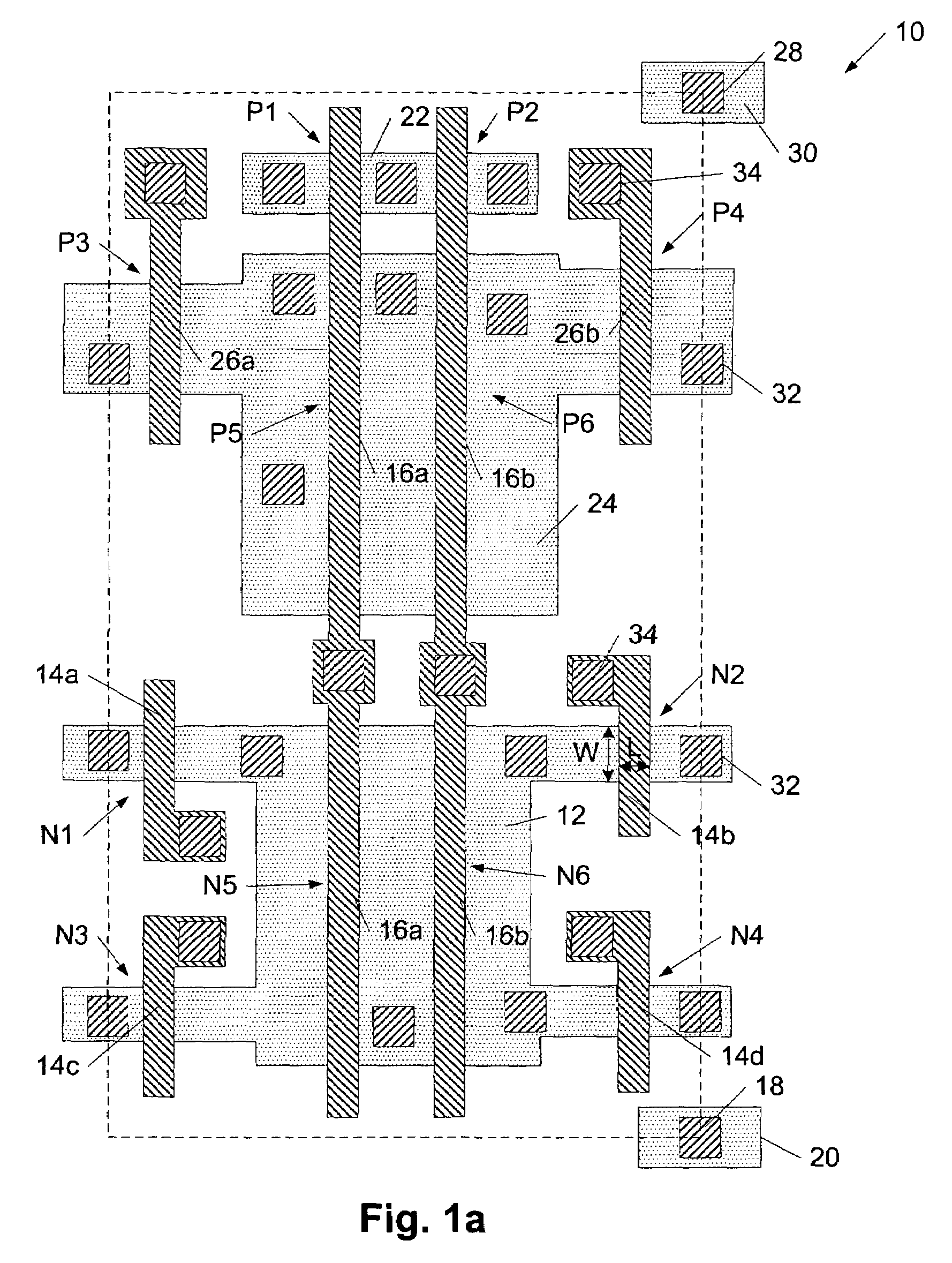
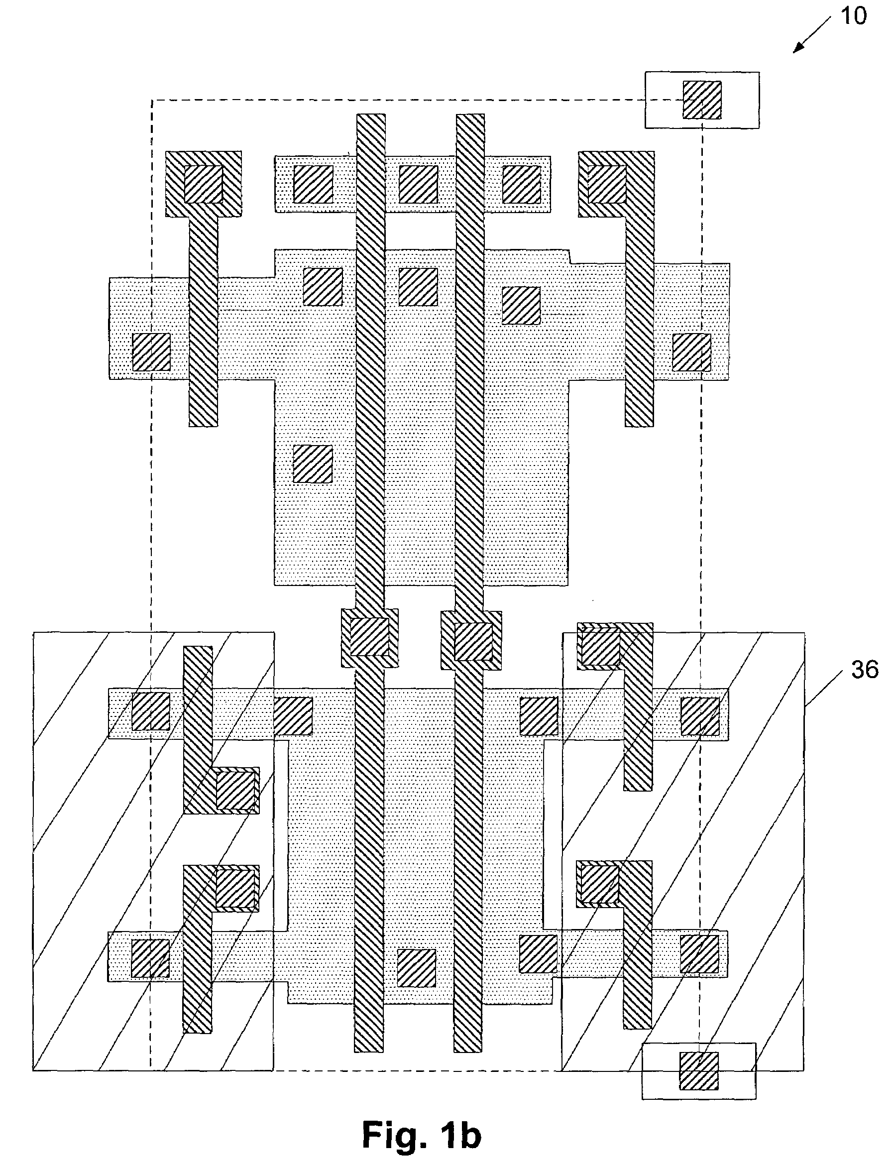
[0023]Turning to the drawings, FIG. 1a illustrates an exemplary plan view of basic cell architecture 10 having a plurality of transistors, which may serve as a repeatable base pattern of fixed layers for a structured ASIC. In particular, basic cell architecture 10 illustrates a layout of a plurality of transistors dimensionally configured and arranged such that when replicated within an array of cells, the plurality of cells form a building block for subsequent formation of logic circuitry and / or memory circuitry with overlying variable layers. The memory circuitry may include any memory technology that can receive written logic values and transmit read logic values that are stored in the interim, such as SRAM, DRAM or non-volatile technologies. The logic circuitry may include any logic circuitry, such as but not limited to NAND gates, NOR gates, XOR gates, AOIs, registers, and flip flops. As noted above, the fixed layers of structured ASIC do not change across a wafer and, thus, ...


PUM


Abstract

A basic cell circuit architecture having plurality of cells with fixed transistors configurable for the formation of logic devices and/or single/dual port memory devices within a structured ASIC is provided. Different configurations of ensuing integrated circuits are achieved by forming variable interconnect layers above the fixed structures. The circuit architecture can achieve interconnection of transistors within a single cell and/or across multiple cells. The interconnection can be configured to form basic logic gates as well as more complex digital and analog subsystems. In addition, each cell contains a layout of transistors that can be variably coupled to achieve a memory device, such as a SRAM device. By having the capability of forming either a logic circuit element, a memory device, or both, the circuit architecture is both memory-centric and logic-centric, and more fully adaptable to modern-day SoCs.

Description

BACKGROUND OF THE INVENTION[0001]1. Field of the Invention[0002]This invention relates to integrated circuits and, more particularly, to cell based integrated circuit architecture that is configurable for the formation of logic devices and / or single / dual port memory devices.[0003]2. Description of the Related Art[0004]The following descriptions and examples are not admitted to be prior art by virtue of their inclusion within this section.[0005]An integrated circuit generally includes the interconnection of various circuit elements. Those circuit elements include transistors, resistors, capacitors, logic gates, flip-flops, registers, etc. In order to achieve functionality, the various circuit elements must be interconnected with attention given to where those elements are relative to each other. In particular, performance of an integrated circuit is affected by where the elements are connected and the interconnect length between elements. As such, optimal performance of circuit eleme...

Claims


Application Information

Patent Timeline
IPC IPC(8): G06F17/50
CPCH01L27/0207H03K19/1735H01L27/1104H01L27/11807H01L27/11G06F2217/64G06F2115/06H10B10/00H10B10/12
Inventor VENKATRAMAN, RAMNATHDILLON, MICHAEL N.GARDNER, DAVID A.MONZEL, III, CARL ANTHONYRAMESH, SUBRAMANIANARMSTRONG, ROBERT C.DELP, GARY SCOTTPETERSON, SCOTT ALLEN
Owner AVAGO TECH INT SALES PTE LTD
Why Eureka
Try Eureka