Radio frequency IC tag and method for manufacturing the same

a radio frequency ic tag and frequency technology, applied in the direction of printed circuit non-printed electric components, instruments, semiconductor/solid-state device details, etc., can solve the problems of difficult communication, reduced antenna efficiency, and short communication distance, so as to achieve maximum antenna efficiency, increase antenna efficiency, and reduce antenna efficiency.

Inactive Publication Date: 2008-07-29
HITACHI LTD
View PDF8 Cites 177 Cited by
  • Summary
  • Abstract
  • Description
  • Claims
  • Application Information

AI Technical Summary

Benefits of technology

[0012]Moreover, a radio frequency IC tag according to the present invention can achieve the maximum antenna efficiency by positioning the power-feeding part equipped with the IC chip at a position where the radiation parts become symmetric in the up and down direction (the vertical direction, i.e., the direction perpendicular to the direction of the antenna current) and also in the right and left direction (the horizontal direction, i.e., the direction of antenna current). However, if a shape of a case for storing the radio frequency IC tag is subject to some constraints, the power-feeding part can be positioned at a position where the radiation parts become asymmetric at least either in the up-and-down direction or in the right-and-left direction. Further, if a shape of the case is subject to some constraints, the radiation part may be provided with one or more openings having an arbitrary shape at an arbitrary position thereof. In another case, the radiation part may be provided with one or more notches having an arbitrary shape at an arbitrary position on the outer circumference thereof. If such a changed antenna is used, the antenna efficiency slightly decreases from the maximum efficiency. However, this antenna efficiency is higher than that of a dipole antenna. Accordingly, if higher priority is given to the convenience of attaching to an object, it is also possible to adopt such a changed antenna.

Problems solved by technology

Therefore, if as shown in FIG. 12B the antenna is cut off in the longitudinal direction to miniaturize the radio frequency IC tag, the antenna efficiency decreases, which causes the communication distance to be shortened, resulting in difficult communications.
In other words, a non-contact IC tag that configures an H type antenna by means of electrostatic capacitive coupling cannot be manufactured by utilizing the known conventional manufacturing processes.

Method used


Image

  • Radio frequency IC tag and method for manufacturing the same
  • Radio frequency IC tag and method for manufacturing the same
  • Radio frequency IC tag and method for manufacturing the same

Examples


first embodiment

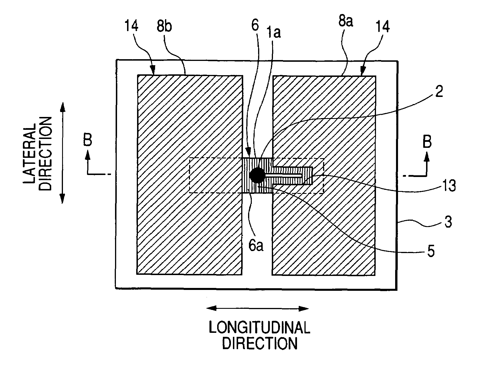
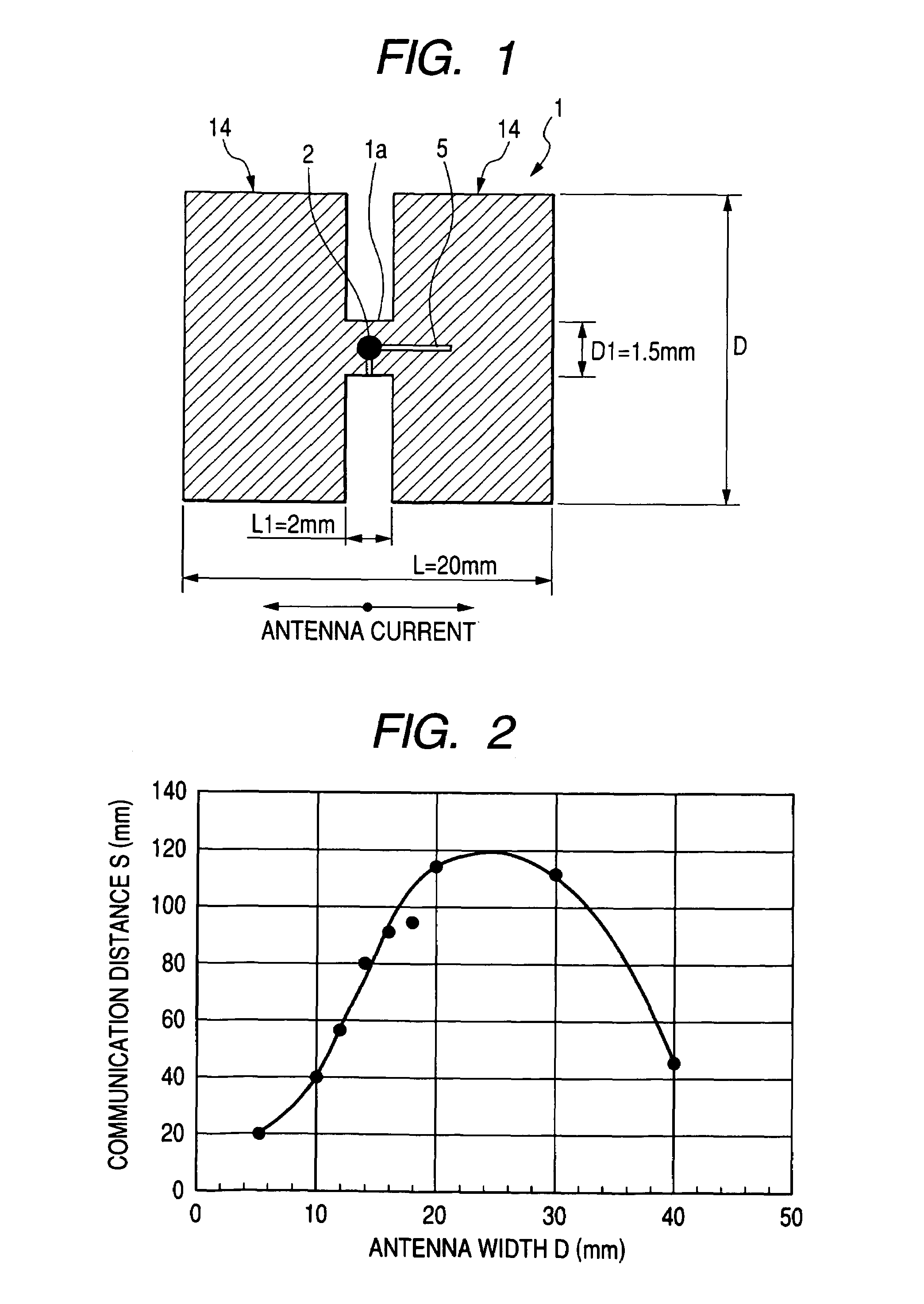
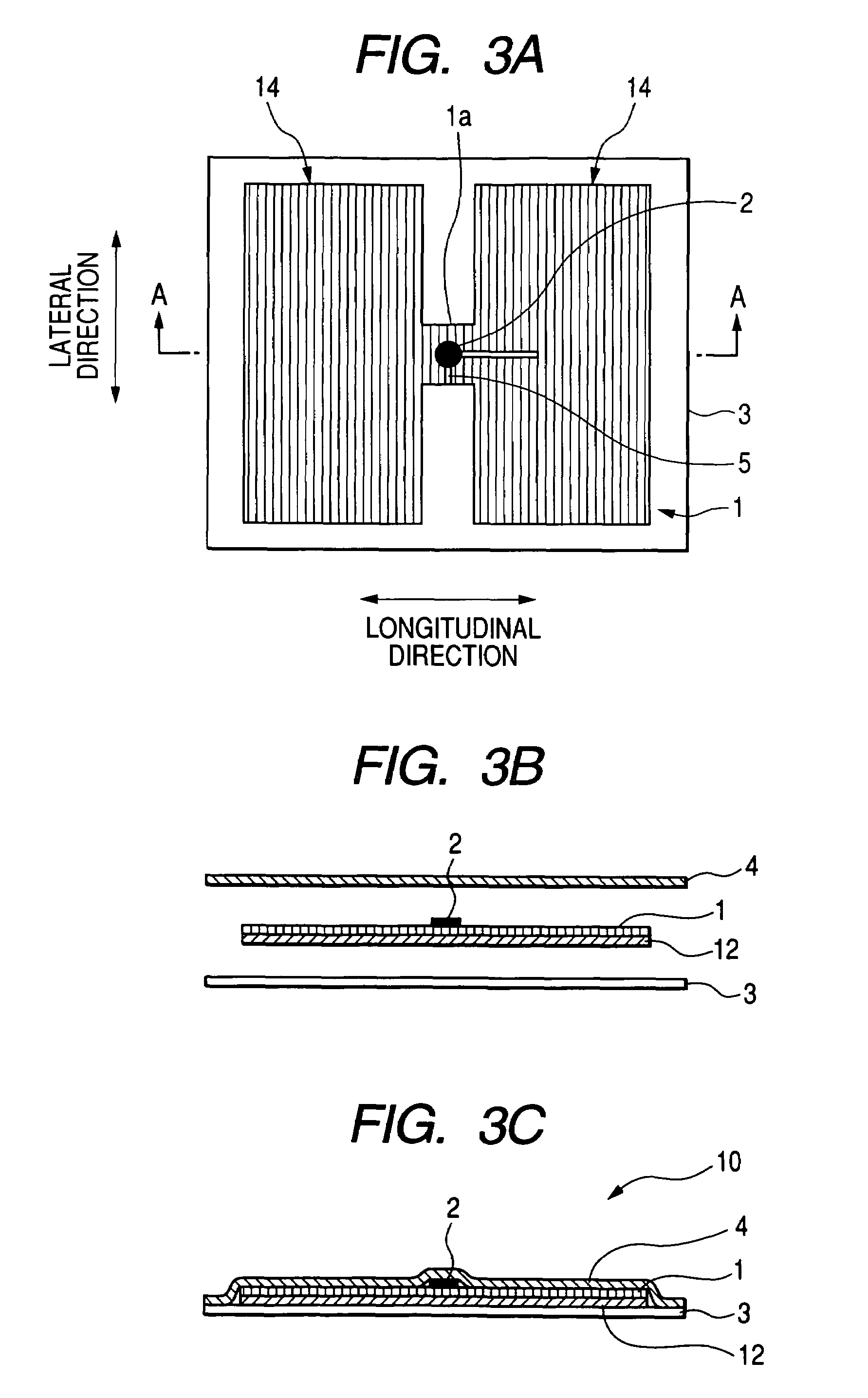
[0027]FIG. 1 is a plan view illustrating an H type antenna used in a radio frequency IC tag according to a first embodiment of the present invention. As shown in FIG. 1, an H type antenna 1 used in the radio frequency IC tag has a so-called H shape in which the antenna width D1 is narrowed in the central part of the antenna forming a constriction 1a extending in a direction of a length L1 while the antenna width D is widened at both side parts (peripheral radiation parts) 14 of the antenna 1 extending in the direction of the length L. In addition, an IC chip 2 is mounted on the central part of the H type antenna 1. The H type antenna 1 functions as a strip antenna. The H type antenna 1 takes preventive measures against electrostatic discharge damage, and performs impedance matching. Therefore, a consecutive key-shaped (or L-shaped) slit 5 is formed in the central part equipped with the IC chip 2 in such a manner that the IC chip 2 is placed across the slit 5, and the terminals of th...

second embodiment

[0049]FIG. 5 is a plan view illustrating an O type (dumbbell or oval type) antenna used in a radio frequency IC tag according to a second embodiment of the present invention. As shown in FIG. 5, an O type antenna 9 having a generally circular or oval shape has a configuration in which the central part 9a between two pieces of semicircular metal foil 15 having a radius of R is connected with rectangular metal foil having a width of D2. The rectangular metal foil part is equipped with the IC chip 2 to form a radio frequency IC tag. When an antenna current flows from the IC chip 2 of the O type antenna 9 having such a shape toward a direction indicated by an arrow in FIG. 5, the maximum current flows in the central part 9a (the part equipped with the IC chip 2 which forms a power-feeding part), and the antenna current then flows toward semicircular parts 15 at both sides, which act as radiation parts. As a result, the electromagnetic energy of the semicircular parts 15 at both sides su...

third embodiment

[0050]What will be described in this embodiment are some variations of radio frequency IC tags in which the shapes of the H type antenna and of the O type antenna described above are changed. In the embodiments described above, the width of the central part of an antenna extending in the longitudinal direction is narrowed to form an H-shaped or O-shaped antenna, and the radio frequency IC tag is equipped with the IC chip in the central part of the antenna. On the contrary, in a radio frequency IC tag according to a third embodiment, a position at which the IC chip is mounted (that is, a constriction) is moved from the central part of the antenna to a desired position so as to form an H type antenna, or an O type antenna, having a changed shape. In another case, the right and left shapes of an H type antenna or of an O type antenna, or the top and bottom shapes of an H type antenna or of an O type antenna, are made asymmetric so as to form the H type antenna, or the O type antenna, h...


PUM

PropertyMeasurementUnit
heightaaaaaaaaaa
lengthaaaaaaaaaa
lengthaaaaaaaaaa

Abstract

A radio frequency IC tag and a manufacturing method for the same includes an IC chip on which information is stored, and an antenna for transmitting the information that is stored on the IC chip. In the antenna, a power-feeding part on which the IC chip is mounted extends along a direction in which an electric current flows. Radiation parts are formed so that the width of the radiation parts becomes wider than that of the power-feeding part with respect to the longitudinal axis of the power-feeding part. The radiation parts extend from the power-feeding part, at both sides thereof, along the direction in which the electric current flows.

Description

CROSS-REFERENCES TO RELATED APPLICATIONS[0001]This application claims priority based on Japanese Patent Application No. 2004-173566, filed Jun. 11, 2004, and Japanese Patent Application No. 2004-345335, filed Nov. 30, 2004, both of which are incorporated herein by reference.BACKGROUND OF THE INVENTION[0002]In recent years, radio frequency IC tags have become widely used for information management and distribution management of commodities, articles, and the like. Moreover, these radio frequency IC tags are also coming into common use for the identification and management of animals. Such radio frequency IC tags usually include a small IC chip on which information is stored, and a small antenna for transmitting information stored in the IC chip by, such as by radio frequency transmission, other electromagnetic energy transmission, or the like, as is known in the art. (See, for example, U.S. Pat. No. 6,617,172 to Usami, and U.S. patent application Ser. No. 10 / 513,995, to Oozeki, filed...

Claims


Application Information

Patent Timeline
Patent Type & Authority Patents(United States)
IPC IPC(8): G08B13/14H01Q1/38H05K3/02G06K19/077H01Q1/22H01Q7/00H01Q9/28H01Q19/00
CPCG06K19/07756G06K19/07786H01Q1/2225H01Q7/00H01Q19/00H01Q9/285Y10T29/49156Y10T29/49155Y10T156/1052G06K19/077
Inventor SAKAMA, ISAOASHIZAWA, MINORU
Owner HITACHI LTD
Why Eureka
Try Eureka