Multi-domain ESD protection circuit structure

a protection circuit and multi-domain technology, applied in the direction of emergency protection arrangements for limiting excess voltage/current, and arrangements responsive to excess voltage, can solve the problems of electrostatic discharge (esd), extreme high voltage development in the vicinity of an integrated circuit, and destruction of the entire integrated circuit, so as to save layout area and improve esd protection performance

Inactive Publication Date: 2008-08-12
TAIWAN SEMICON MFG CO LTD
View PDF10 Cites 39 Cited by
  • Summary
  • Abstract
  • Description
  • Claims
  • Application Information

AI Technical Summary

Benefits of technology

[0008]The preferred embodiment of the present invention is devised to provide a multi-domain ESD protection circuit structure. The present invention uses an existing internal circuit's power lines as ESD buses. The ESD protection performance is improved since the ESD current flows through fewer ESD protection devices. The layout area is saved since no additional ESD buses are needed.

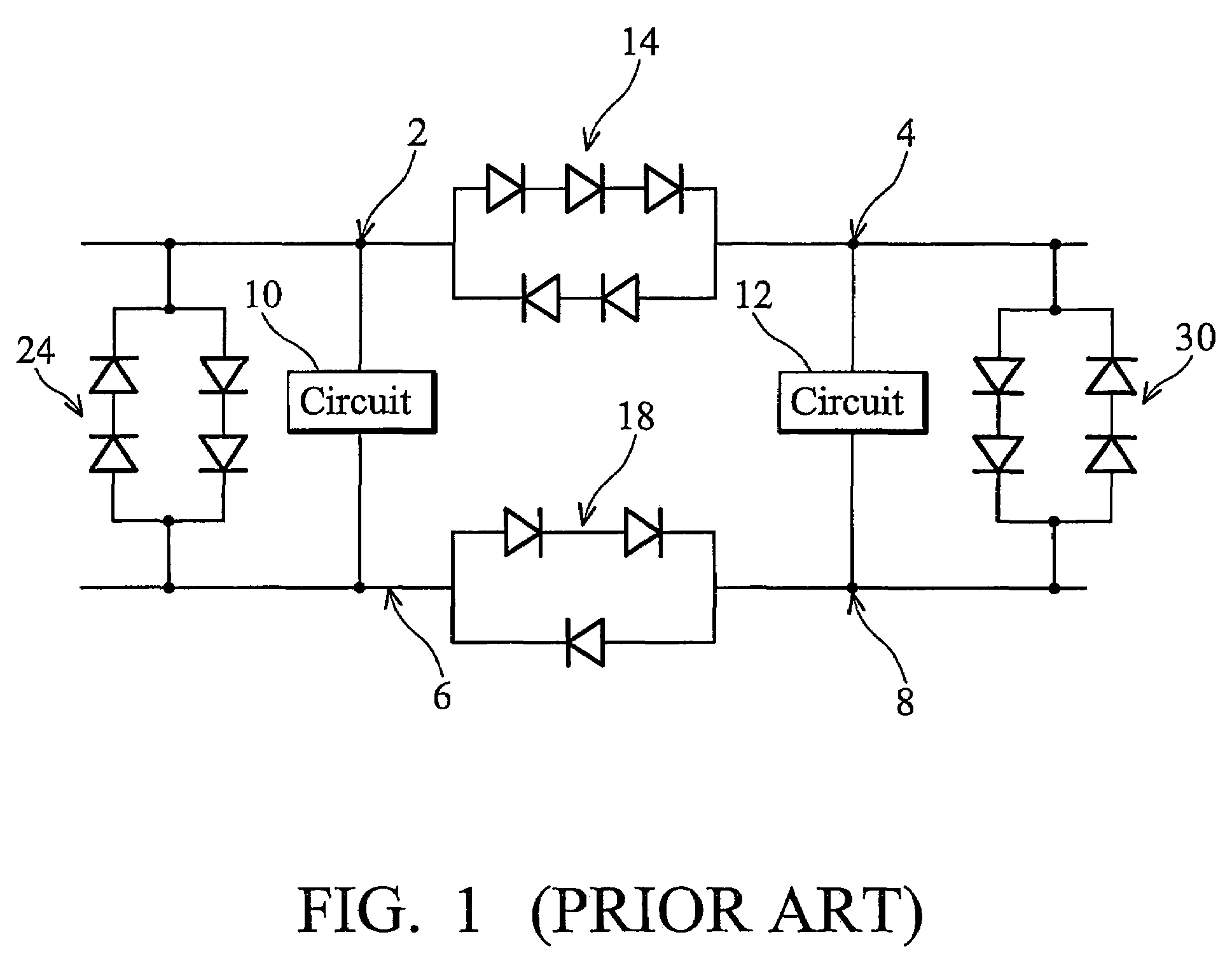
Problems solved by technology

It is well known that extremely high voltages can develop in the vicinity of an integrated circuit due to the build-up of static charge.
ElectroStatic Discharge (ESD) is a serious problem for semiconductor devices since it has the potential to destroy the entire integrated circuit.
The duration of the ESD transient is very short, typically in the order of nanoseconds, so that the conventional circuit breakers do not react quickly enough to provide adequate protection.
However, the separation of the power lines creates more power lines that are subject to ESD.

Method used


Image

  • Multi-domain ESD protection circuit structure
  • Multi-domain ESD protection circuit structure
  • Multi-domain ESD protection circuit structure

Examples


Embodiment Construction

[0017]The making and using of the presently preferred embodiments are discussed in detail below. It should be appreciated, however, that the present invention provides many applicable inventive concepts that can be embodied in a wide variety of specific contexts. The specific embodiments discussed are merely illustrative of specific ways to make and use the invention, and do not limit the scope of the invention.

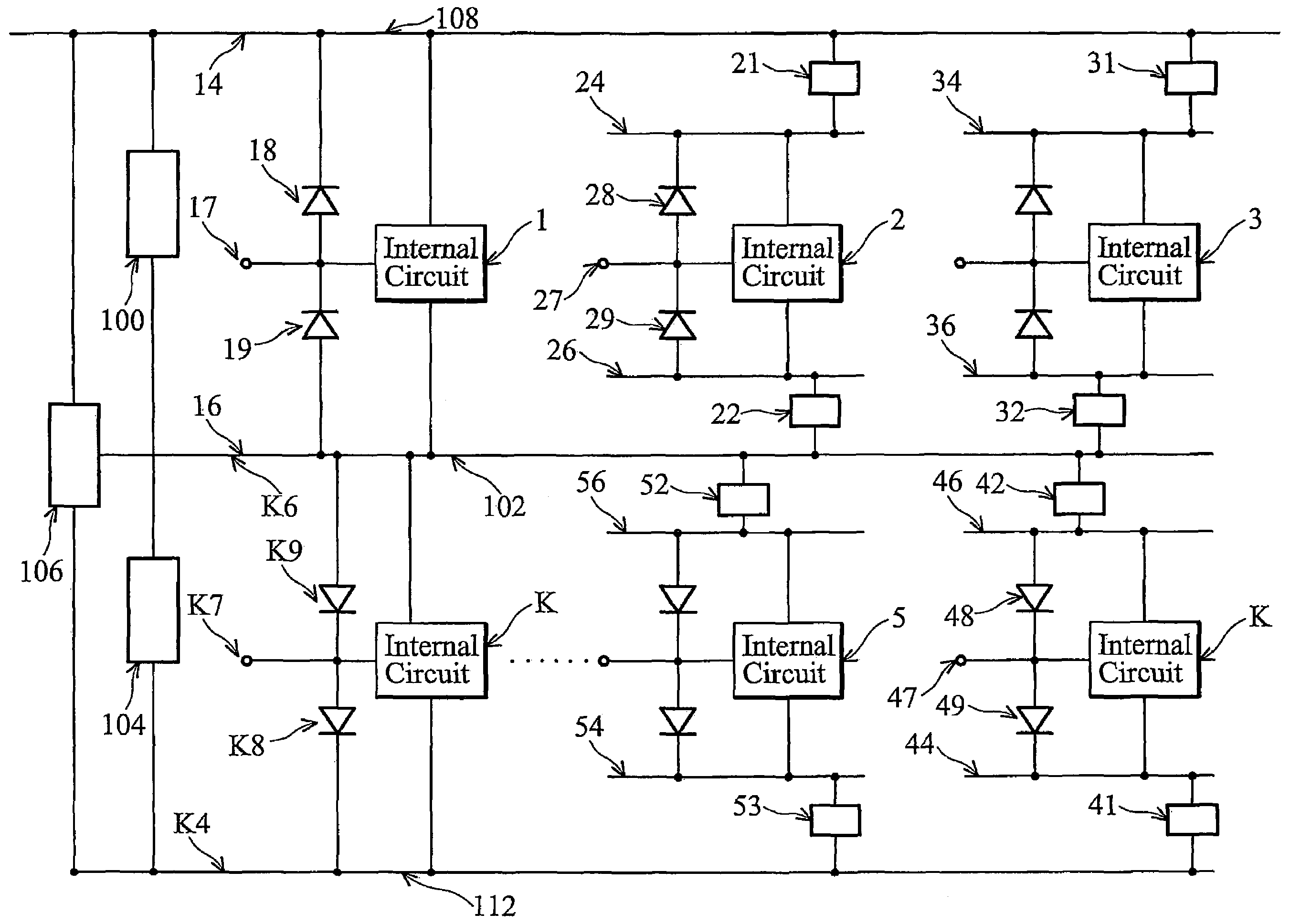
[0018]The preferred embodiment of the multi-domain ESD protection circuit will be described. Various aspects of the present invention will be presented. An application of the present invention will then be explained.

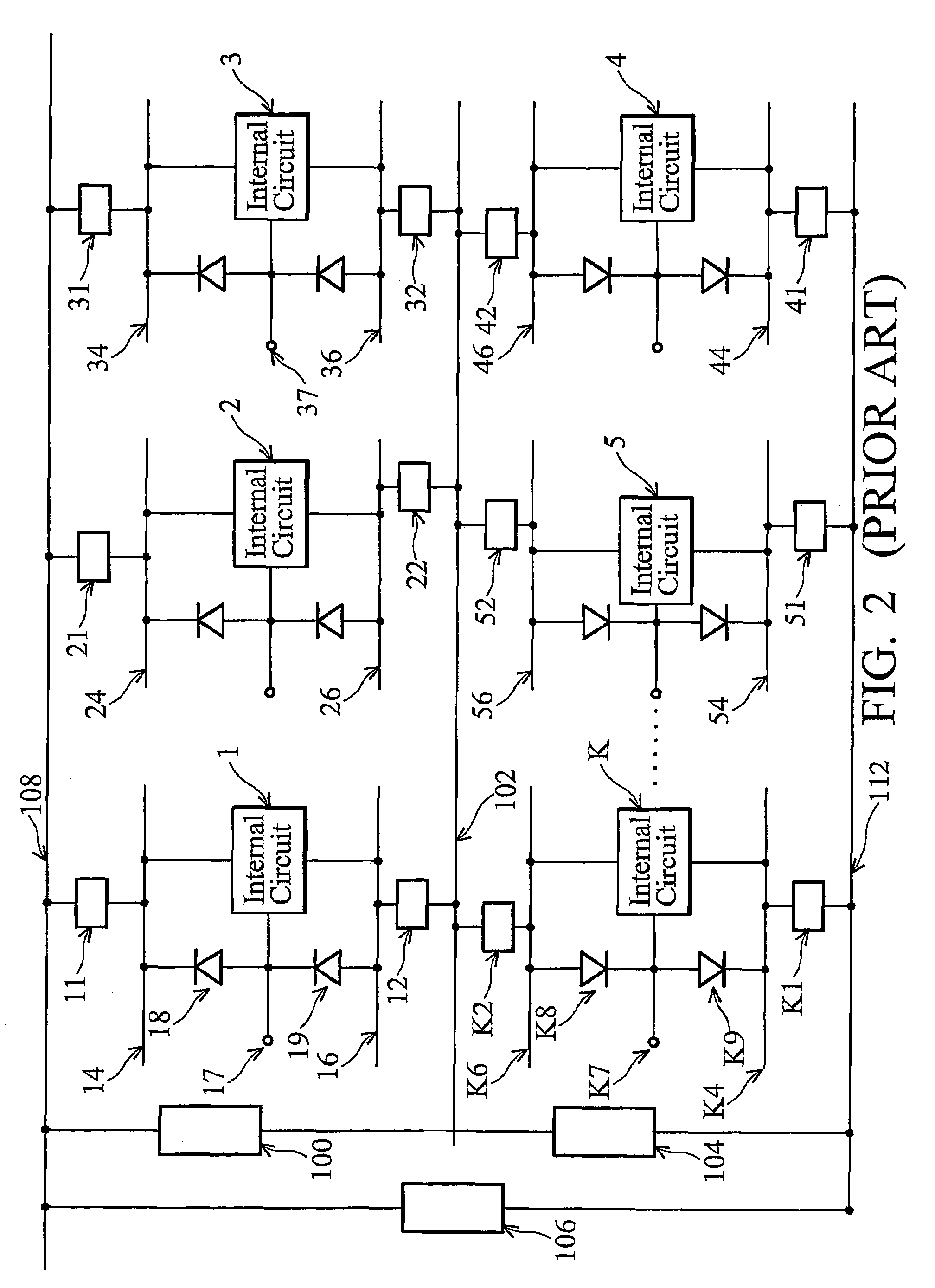
[0019]For the convenience of the description, multiple internal circuits are used. Each internal circuit is denoted by a number and the elements of the internal circuits are denoted by like numbers prefixed by the internal circuit number. For example, the VDD power line is represented by 4, so that the VDD power line of the internal circuit 1 is 14, the VDD power ...


PUM


Abstract

A multi-domain ESD protection circuit structure is described. The preferred embodiment of the present invention selects power lines of an internal circuit as ESD buses. The power lines of the remaining internal circuits are coupled with the ESD buses through the ESD connection cells. In another embodiment of the preferred invention, the VDD power line from one internal circuit and the VSS power line from another circuit are selected as ESD buses. In yet another embodiment, either a VDD power line or a VSS power line of an internal circuit is selected as an ESD bus.

Description

FIELD OF INVENTION[0001]This invention relates generally to an ESD protection circuit and more particularly to ESD buses used by power domains.BACKGROUND[0002]It is well known that extremely high voltages can develop in the vicinity of an integrated circuit due to the build-up of static charge. A high potential may be generated to an input or output buffer of an integrated circuit, which may occur by a person simply touching a package pin, which is in electrical contact with an input or output buffer of the integrated circuit. When the electrostatic is discharged, a high current is produced at the package nodes of the integrated circuit. ElectroStatic Discharge (ESD) is a serious problem for semiconductor devices since it has the potential to destroy the entire integrated circuit.[0003]The duration of the ESD transient is very short, typically in the order of nanoseconds, so that the conventional circuit breakers do not react quickly enough to provide adequate protection. For this r...

Claims


Application Information

Patent Timeline
Patent Type & Authority Patents(United States)
IPC IPC(8): H02H9/00H01L23/60H01L27/02H02H3/20
CPCH01L27/0292H01L27/0251
Inventor HUANG, SHAO-CHANGAN, CHI-DISONG, MING-HSIANG
Owner TAIWAN SEMICON MFG CO LTD
Why Eureka
Try Eureka