
Laser patterning of light emitting devices

a technology of light emitting device and laser patterning, which is applied in the direction of photomechanical treatment originals, instruments, manufacturing tools, etc., can solve the problems of reducing affecting the efficiency of conventional leds, and inability to emit all ligh

Active Publication Date: 2008-09-02
CREE INC
View PDF55 Cites 36 Cited by
  • Summary
  • Abstract
  • Description
  • Claims
  • Application Information

AI Technical Summary

Problems solved by technology

The efficiency of conventional LEDs may be limited by their inability to emit all of the light that is generated by their active layer.
Because of this phenomenon, much of the light generated by conventional LEDs does not emit, degrading its efficiency.

Method used


Image

  • Laser patterning of light emitting devices
  • Laser patterning of light emitting devices
  • Laser patterning of light emitting devices

Examples


examples

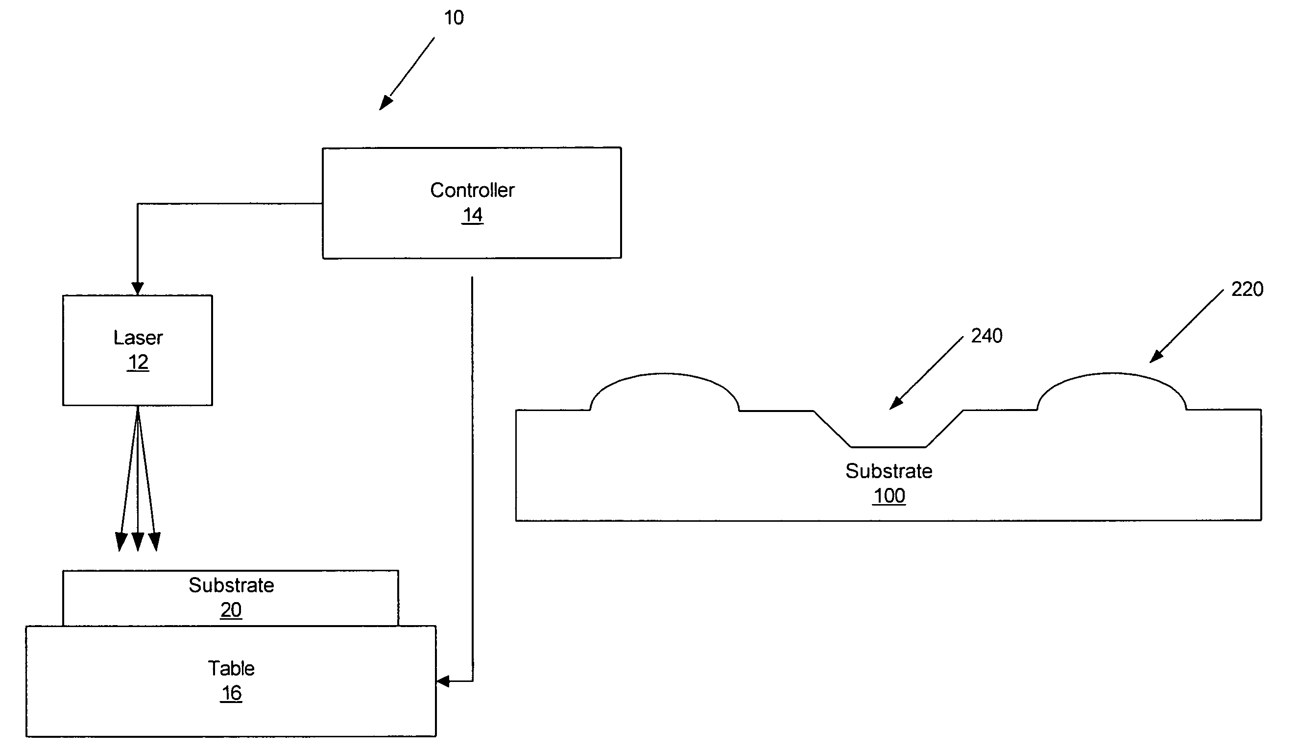
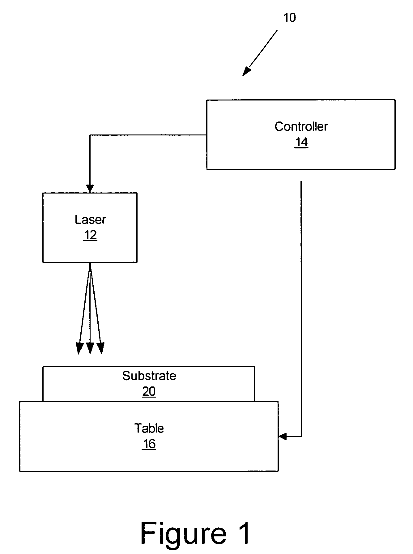
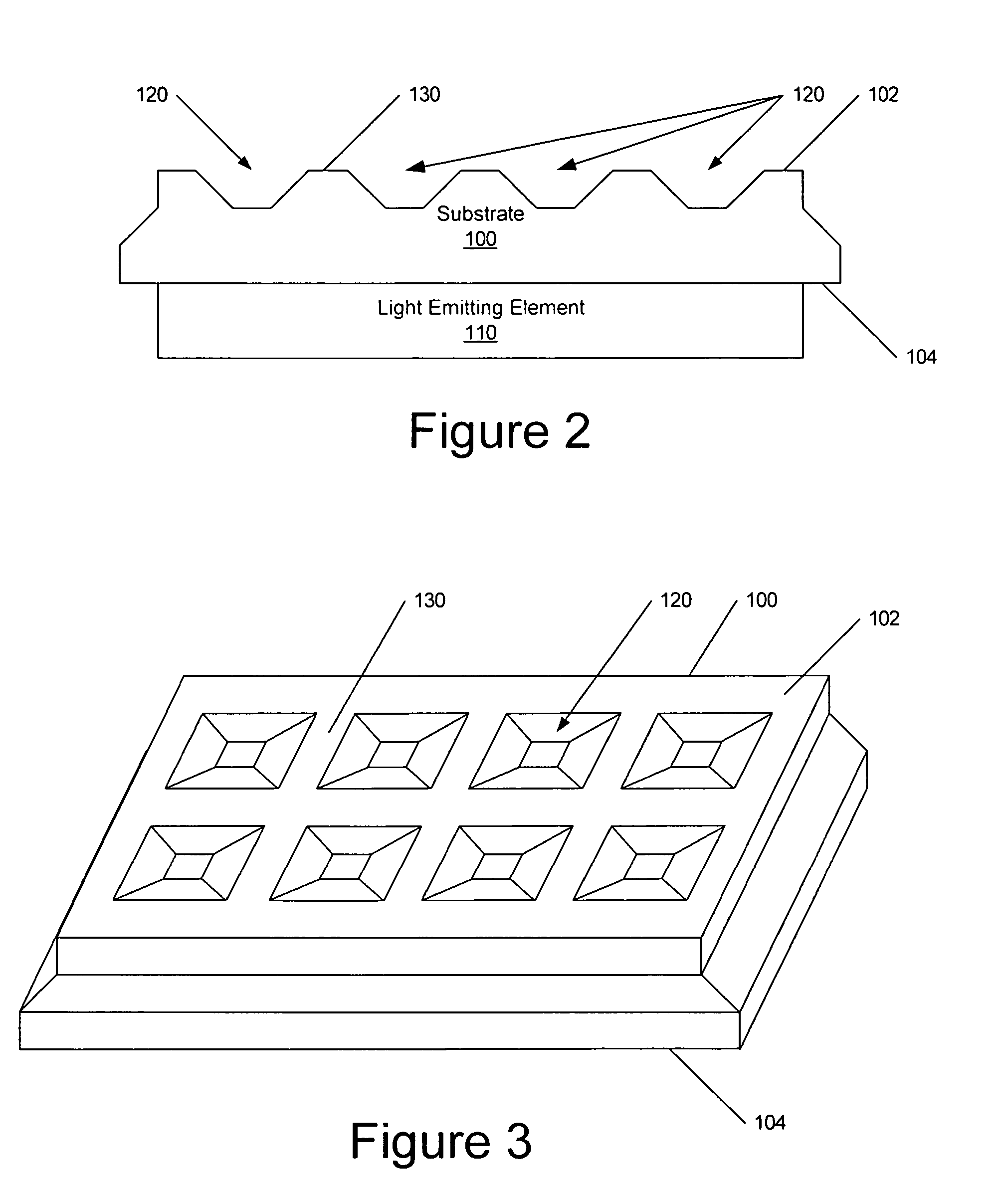
[0073]An excimer laser operating at 308 nm and using mask projection optics that project a 2 mm×2 mm field was used on a wafer. Using a step and repeat sequence, geometric patterns were laser scribed into the backside of a SiC LED wafer approximately 1 μm deep using 5 pulses at approximately 4.2 J / pulse. Ground control regions were left between the laser scribed regions of the wafer. Subsequent to the laser process, the wafers were aggressively etched in a RIE tool to remove any light absorbing material generated by the laser process. Because the RIE process is anisotropic, the morphology change induced by the laser was maintained. Initial test patterns were 10 μm squares, 15 μm circles, 20 μm crosses and 20 μm stars. Die from the square patterned areas showed the largest increase in light output versus die from the control region. Approximately a 20% increase was provided by a double pass interleaved square pattern over the die from the control regions.

[0074]FIGS. 14A and 15A are i...


PUM

PropertyMeasurementUnit
wavelengthsaaaaaaaaaa

Abstract

Light extraction features are provided for a light emitting device having a substrate and a semiconductor light emitting element on the substrate by shaping a surface of a layer of semiconductor material utilizing a laser to define three dimensional patterns in the layer of semiconductor material. The layer of semiconductor material may be the substrate. In particular embodiments of the present invention, the surface of the layer of semiconductor material is shaped by applying laser light to the layer of semiconductor material at an energy sufficient to remove material from the layer of semiconductor material. The laser light may also by applied in a blanket manner at a level below the ablation threshold. The application of laser light to the layer of semiconductor material may be followed by etching the substrate. The layer of semiconductor material may be anisotropically etched. A mask could also be patterned utilizing laser light and the layer of semiconductor material etched using the mask. Light emitting devices have three dimensional patterns in a layer of semiconductor material of the device are also provided.

Description

FIELD OF THE INVENTION[0001]This invention relates to semiconductor light emitting devices and fabricating methods therefor.BACKGROUND OF THE INVENTION[0002]Semiconductor light emitting devices, such as Light Emitting Diodes (LEDs) or laser diodes, are widely used for many applications. As is well known to those having skill in the art, a semiconductor light emitting device includes a semiconductor light emitting element having one or more semiconductor layers that are configured to those having skill in the art, a light emitting diode or laser diode, generally includes a diode region on a microelectronic substrate. The microelectronic substrate may be, for example, gallium arsenide, gallium phosphide, alloys thereof, silicon carbide and / or sapphire. Continued developments in LEDs have resulted in highly efficient and mechanically robust light sources that can cover the visible spectrum and beyond. These attributes, coupled with the potentially long service life of solid state devic...

Claims


Application Information

Patent Timeline
Patent Type & Authority Patents(United States)
IPC IPC(8): H01L21/311B29D11/00G03F1/00B23K26/00B23K26/06B23K26/40H01L21/027H01L21/04H01L33/00H01L33/20H01L33/32
CPCB23K26/0656B23K26/4075B23K26/408H01L33/0095H01L33/20Y10S438/94H01L33/32B23K2201/40B23K26/066B23K26/40B23K2101/40B23K2103/50B23K2103/52
Inventor DONOFRIO, MATTHEW
Owner CREE INC
Learn More