Digital parallel electron beam lithography stamp

a technology of electron beam and electron beam, applied in the field of digital parallel electron beam lithography stamp, can solve the problems of limiting the speed of production, affecting the efficiency of production, and limiting the technique, so as to improve the environmental control, improve the degree of addressability, and improve the effect of density array

Inactive Publication Date: 2008-09-16
MOUTTET BLAISE LAURENT
View PDF24 Cites 0 Cited by
  • Summary
  • Abstract
  • Description
  • Claims
  • Application Information

AI Technical Summary

Benefits of technology

[0009]The present invention provides a Parallel Electron Beam Lithography Stamp (PEBLS) that includes controls and wiring allowing for a high degree of addressability in high density arrays of emission tips. Improved environmental control may be maintained during lithography performed by the PEBLS by forming the emission tips within a cell of a substrate in which a periphery of the cell contacts a target to be processed.

Problems solved by technology

However, these techniques are limited by the wavelengths of the light used and fabrication below 100 nm is problematic.
Electron and ion beam lithography are alternative techniques capable of providing finer resolution but which typically use a serial scanning process that limits the speed of production.
In addition, the use of masks for optical lithography and the required low pressure environmental control for e-beam lithography induces a high cost to modem fabrication processes.
However, in repeated use, the stamp structure of the mold may be subject to erosion or soiling over time that can negatively impact the achievable resolution so that nanometer resolution patterning becomes impossible or inconsistent and high volume mass production becomes problematic.
However, scanning probe lithography is also a serial process and is therefore too time consuming to be employed in large scale fabrication.
However, in order to control individual electron emitting tips in a large density array, wiring traditionally becomes a limiting factor and an effective parallel e-beam nanofabrication tool useful in mass production of a wide array of nanostructures, materials, or chemicals has yet to be developed.

Method used


Image

  • Digital parallel electron beam lithography stamp
  • Digital parallel electron beam lithography stamp
  • Digital parallel electron beam lithography stamp

Examples


Embodiment Construction

I. Manufacturing of Digital PEBLS

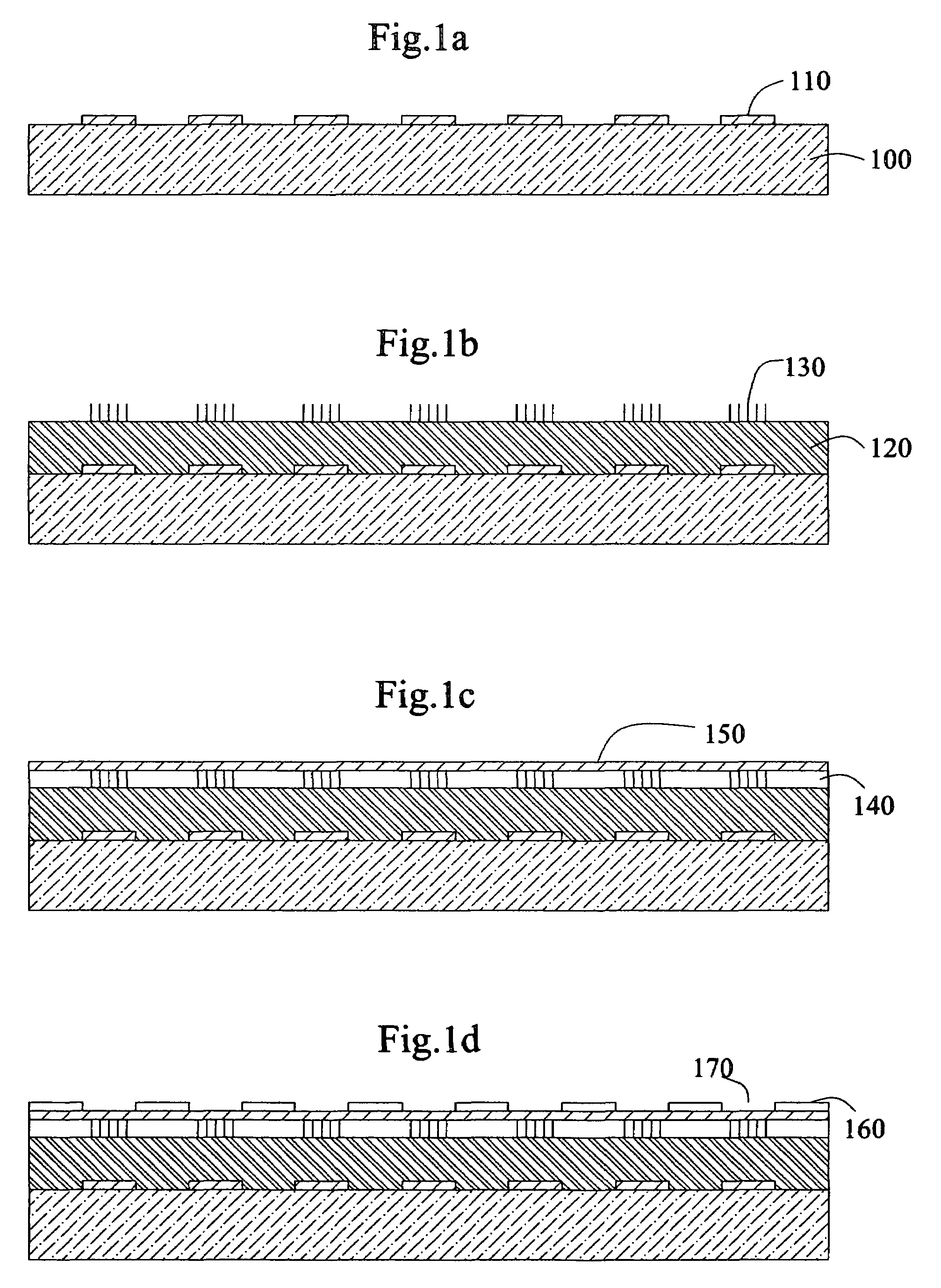
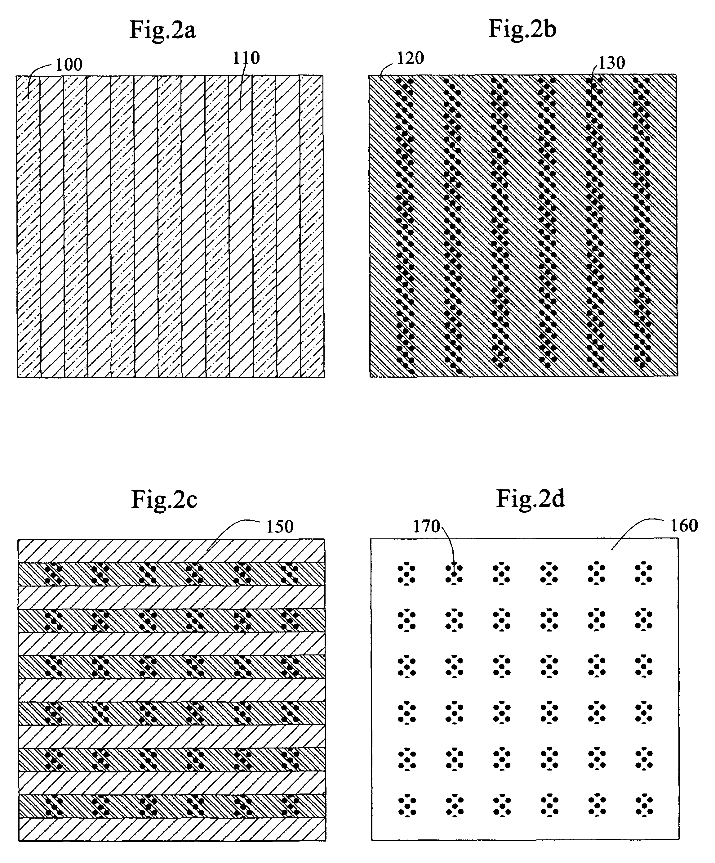
[0020]FIG. 1a-1d illustrate the side view of one embodiment for manufacturing the Parallel Electron Beam Lithography Stamp (PEBLS). FIG. 2a-2d illustrate the top view of this embodiment for manufacturing the PEBLS.

[0021]In FIGS. 1a and 2a, an insulated substrate 100 is provided upon which a first wiring pattern including parallel conductive wires 110 is formed using either conventional optical lithographic approaches or, for finer resolution patterning, using e-beam lithography, nanoimprint lithography, dip pen nanolithography, etc. The material of the wiring pattern includes catalytic material such as metallic nanoparticles of Fe, Ni, Co, or Mo.

[0022]In FIGS. 1b and 2b, an anodic aluminum oxide (AAO) template 120 is formed on the substrate 100 with the wiring pattern using known techniques such as disclosed by the articles of Kim et al. “Growth of carbon nanotubes with anodic aluminum oxide formed on the catalytic metal-coated Si substrate” (Diamond...


PUM


Abstract

An array of vertically aligned electron emitting nanotips such as multiwall carbon nanotubes are formed for use as a lithographic stamp. Crosswire addressing is used to generate electron emission from particular nanotips within the array. The nanotip array may be used to cure a resist, produce localized electrochemical reactions, establish localized electrostatic charge distributions, or perform other desirable coating or etching process steps so as to create nanoelectronic circuitry or to facilitate molecular or nanoscale processing.

Description

CROSS-REFERENCE TO RELATED APPLICATIONS[0001]This application is related to the following co-pending patent application, which is incorporated by reference in its entirety: U.S. application Ser. No. 11 / 395,238, entitled “Parallel Electron Beam Lithography Stamp (PEBLS),” filed Apr. 3, 2006.FIELD OF THE INVENTION[0002]The present invention pertains to a tool and method used to form nanostructures or nano-structural features and is applicable to the fields of electronic device fabrication, material processing, chemical processing, and biological processing at nanometer dimensions.BACKGROUND OF THE INVENTION[0003]Small scale fabrication has been dominated over the past 40 years by lithography techniques that employ radiation in the form or visible or ultraviolet light. However, these techniques are limited by the wavelengths of the light used and fabrication below 100 nm is problematic. Electron and ion beam lithography are alternative techniques capable of providing finer resolution b...

Claims


Application Information

Patent Timeline
Patent Type & Authority Patents(United States)
IPC IPC(8): G21K5/00
CPCB82Y10/00B82Y40/00H01J37/3177H01J2237/0635H01J2237/31786H01J2237/2002H01J2237/30438H01J2237/31754H01J2237/182
Inventor MOUTTET, BLAISE LAURENT
Owner MOUTTET BLAISE LAURENT
Why Eureka
Try Eureka