Microlens for use with a solid-state image sensor and a non-telecentric taking lens

a microlens and solid-state image sensor technology, applied in the field of image sensing technology, can solve the problems of ccd imagers that require specialized facilities, ccd imagers that consume a substantial amount of power, and complex ccd systems, and achieve the effect of maximizing the light sensitivity of each pixel

Active Publication Date: 2008-09-23
SK HYNIX INC
View PDF13 Cites 22 Cited by
  • Summary
  • Abstract
  • Description
  • Claims
  • Application Information

AI Technical Summary

Benefits of technology

[0027]A fifth aspect of the present invention is an imaging system. The imaging system includes a two-dimensional array of photosensors, each photosensor having a center point; a non-telecentric lens positioned over the two-dimensional array of photosensors; and a two-dimensional array of microlenses positioned over the two-dimensional array of photosensors, each microlens being associated with a corresponding photosensor, each microlens having a center point. The microlens is positioned over the corresponding photosensor such that a center point of a microlens is offset from a center point of a corresponding photosensor, each offset having an amount and a direction such that the amounts and directions spatially vary across the two-dimensional array of photosensors. The spatial variation is determined based on optical characteristics of the non-telecentric lens and optical properties of the two-dimensional array of photosensors and the microlenses such that light sensitivity of each pixel is maximized.

Problems solved by technology

First, CCD imagers require specialized facilities, which are dedicated exclusively to the fabrication of CCDs.
Second, CCD imagers consume a substantial amount of power, since they are essentially capacitive devices, which require external control signals and large clock swings to achieve acceptable charge transfer efficiencies.
Third, CCD imagers require several support chips to operate the device, condition the image signal, perform post processing, and generate standard video output.
This need for additional support circuitry makes CCD systems complex.
Finally, CCD systems require numerous power supplies, clock drivers and voltage regulators, which not only further increase the complexity of the design, but also demand the consumption of additional significant amounts of power.
Despite the improvement in effective fill factor using cylindrically shaped microlenses, there are negative performance factors, which are attributable to use of rectangular-shaped image sensing areas and cylindrically-shaped microlenses.
This ineffectiveness further involves light that is scattered and / or reflected and which ultimately arrives at the lenses 203 at oblique angles.
This second type of crosstalk occurs between pixels of different colors and is referred to in the art as “color crosstalk.” Color crosstalk leads to color distortion and is largely caused by the fact that silicon-based photodiodes have a wavelength-dependent photon absorption response.
In particular, color distortion can be significant for image arrays that use rectangular-shaped image sensing areas together with an RGB Bayer pattern color filter.
This difference in green pixel responsivity results in color distortion.
Finally, yet another problem that is observed when neighboring image-sensing areas are too closely positioned, is a decrease in spatial resolution.
The lower the MTF, the less capable an imaging device is at picking up the fine detail and contrast in the object that is being imaged.
However, the maximum achievable fill factor is limited by the CMOS fabrication design rules between photodiodes and MOS transistors.
As a result, the fill factor is reduced and the sensor performance is degraded.

Method used


Image

  • Microlens for use with a solid-state image sensor and a non-telecentric taking lens
  • Microlens for use with a solid-state image sensor and a non-telecentric taking lens
  • Microlens for use with a solid-state image sensor and a non-telecentric taking lens

Examples


Embodiment Construction

[0051]The present invention will be described in connection with preferred embodiments; however, it will be understood that there is no intent to limit the present invention to the embodiments described herein. On the contrary, the intent is to cover all alternatives, modifications, and equivalents as may be included within the spirit and scope of the present invention as defined by the appended claims.

[0052]For a general understanding of the present invention, reference is made to the drawings. In the drawings, like reference have been used throughout to designate identical or equivalent elements. It is also noted that the various drawings illustrating the present invention are not drawn to scale and that certain regions have been purposely drawn disproportionately so that the features and concepts of the present invention could be properly illustrated.

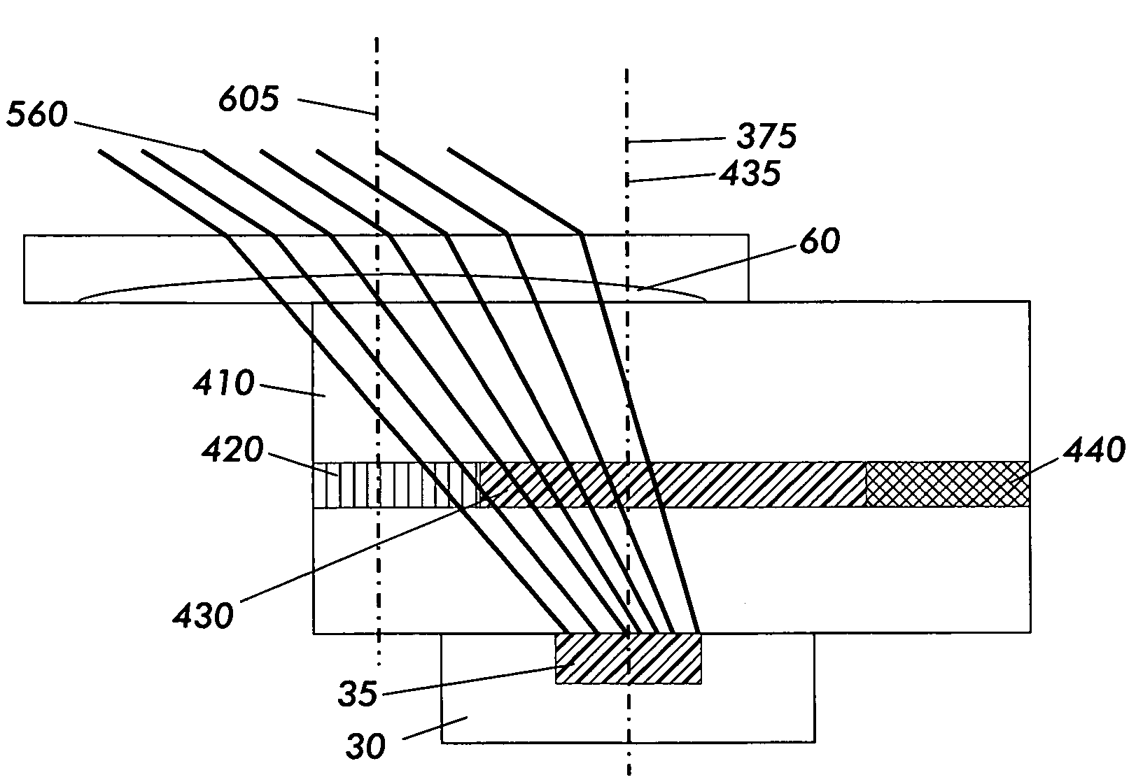
[0053]As noted above, when using a non-telecentric lens, the incident light encounters the pixel site at large angles, which can ad...


PUM


Abstract

An imager includes a two-dimensional array of photosensors, each photosensor having a center point. A non-telecentric lens is positioned over the two-dimensional array of photosensors, and a two-dimensional array of microlenses is positioned over the two-dimensional array of photosensors. Each microlens is associated with a corresponding photosensor, and each microlens has a center point. A color filter array is positioned over the two-dimensional array of photosensors. The color filter array includes a plurality of color filter areas. Each color filter area is associated with a corresponding photosensor and has a center point. A layer of transmissive apertures is further positioned over the two-dimensional array of photosensors. Each aperture is associated with a corresponding photosensor and having a center point. The microlens is positioned over the corresponding photosensor such that the center point of the microlens is offset from the center point of the corresponding photosensor. The color filter area is positioned over the corresponding photosensor such that the center point of the color filter area is offset from the center point of the corresponding photosensor. Finally, the aperture is positioned over the corresponding photosensor such that the center point of the aperture is offset from the center point of the corresponding photosensor.

Description

PRIORITY INFORMATION[0001]This application claims priority from U.S. Provisional Patent Application, Ser. No. 60 / 417,982, filed on Oct. 11, 2002. The entire contents of U.S. Provisional Patent Application, Ser. No. 60 / 417,982 are hereby incorporated by reference.FIELD OF THE PRESENT INVENTION[0002]The present invention relates generally to image sensing technology. More specifically, the present invention relates to a CMOS image sensor that uses shifted microlenses, color filter areas, and apertures to increase the light collection efficiency of a photosensor or photodiode as well as decreasing color signal crosstalk between adjacent pixels.BACKGROUND OF THE PRESENT INVENTION[0003]Conventionally, imaging technology has been centered around charge coupled device (CCD) image sensors. However, recently, CMOS imaging technology has become increasingly the technology of choice. There are a variety of reasons for this progression.[0004]First, CCD imagers require specialized facilities, wh...

Claims


Application Information

Patent Timeline
Patent Type & Authority Patents(United States)
IPC IPC(8): H01J3/14G06T9/00H01L27/146H01L31/0232H04N5/225H04N7/26
CPCG06T9/00H01L27/14601H01L27/14623H01L27/14645H01L27/14667H01L27/14627H01L31/0232
Inventor DROWLEY, CLIFFORD I.WANG, CHIN-CHUN
Owner SK HYNIX INC
Why Eureka
Try Eureka