Body biasing structure of SOI

a body biasing and soi technology, applied in the direction of semiconductor devices, electrical apparatus, transistors, etc., can solve the problems of increasing the potential of the body, undesired operation, and lowering the drain voltage, so as to suppress the floating body effect

a body biasing and soi technology, applied in the direction of semiconductor devices, electrical apparatus, transistors, etc., can solve the problems of increasing the potential of the body, undesired operation, and lowering the drain voltage, so as to suppress the floating body effect

US7432552B2Active Publication Date: 2008-10-07SEOUL NAT UNIV R&DB FOUND +1

Image

  • Body biasing structure of SOI
  • Body biasing structure of SOI
  • Body biasing structure of SOI

Examples


Embodiment Construction

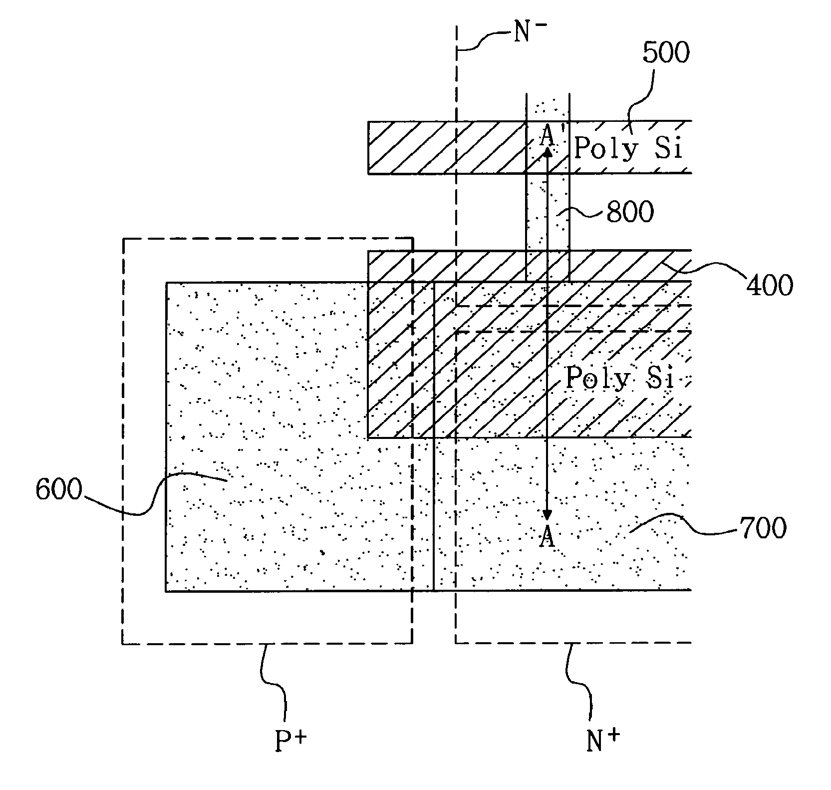
[0042]A body biasing structure of some embodiments includes an SOI substrate; an active region, which is comprised, in the SOI substrate, of a body biasing contact region, a common active region connected to the body biasing contact region, and a device active region connected to the common active region; a field region, which defines the active region in the SOI substrate; a first conducting layer, which is formed on an insulating layer over both one part of the body biasing contact region and one part of the common active region; a second conducting layer, which is formed on an insulating layer over the device active region; a source region, which is formed in the other part of the common active region, over which the first conducting layer is not formed; a common source / drain region, which is formed between the first conducting layer and the second conducting layer; and a body region, which is formed in the active region, where the source region and the common source / drain region...


PUM


Abstract

A body biasing structure of devices connected in series on an SOI substrate is provided. According to some embodiments, the shallow junction of common source / drain regions enables all devices to bias by only one body contact on an SOI substrate like a conventional bulk MOSFET, and the floating body effect on an SOI substrate can be prevented.

Description

CROSS REFERENCE TO RELATED APPLICATION[0001]This application claims priority under 35 U.S.C. § 119 of Korean Patent Application 2005-0050107, filed on Jun. 11, 2005, the entire contents of which are hereby incorporated by reference.BACKGROUND[0002]1. Technical Field[0003]The present invention relates to a body biasing structure for SOI (Silicon-On-Insulator) devices, and more specifically to a body biasing structure of devices connected in series on an SOI substrate.[0004]2. Description of Related Art[0005]SOI technology, which consists of forming a single-crystal-silicon layer on an insulator layer and then forming devices on the silicon layer, has been utilized recently to cope with increasing demands for faster, less power consuming and more highly integrated semiconductor integrated circuits.[0006]SOI technology can decrease the electrical resistance between devices and increase their heat efficiency, and it is useful for high-speed semiconductor devices with small electrical po...

Claims


Application Information

Patent Timeline
07 Oct 2008
Publication
US7432552B2
IPC
H01L27/01
CPC
H01L29/78615; H01L21/18
Inventors
PARK, BYUNG-GOOK; KIM, TAE-HOON