Integration structure and making method of insulator silicon radio frequency integrated circuit

A radio frequency integrated circuit, silicon-on-insulator technology, applied in the direction of circuit, semiconductor/solid-state device manufacturing, electrical components, etc., can solve the problem of damaging radio frequency characteristics

Inactive Publication Date: 2005-12-07
INST OF MICROELECTRONICS CHINESE ACAD OF SCI
View PDF0 Cites 3 Cited by
  • Summary
  • Abstract
  • Description
  • Claims
  • Application Information

AI Technical Summary

Problems solved by technology

The compatibility of the process and the balance of performance have become the most important issues in the design. Among them, LDMOS simultaneously obtains a high cut-off frequency (f T ) and source-drain breakdown voltage (BV DS ), inductors on high-loss silicon substrates to obtain a high quality factor (Q), are technical challenges that must be faced; in order to fu...

Method used


Image

  • Integration structure and making method of insulator silicon radio frequency integrated circuit

Examples


Embodiment Construction

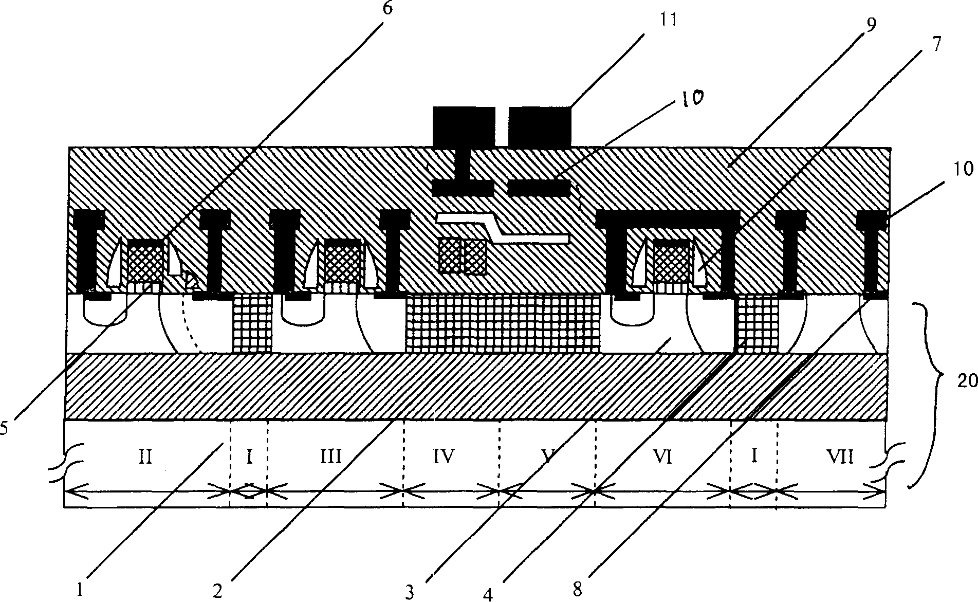
[0035] see figure 1 As shown, the present invention is an integrated structure for silicon-on-insulator radio frequency integrated circuits, which can be divided into device isolation region I, lateral diffusion field effect transistor region II, n-type field effect transistor region III, inductance region IV, capacitance region V, Varactor area VI and diffusion layer resistance area VII 8 areas, characterized in that, including:

[0036] A silicon-on-insulator substrate 20, the silicon-on-insulator substrate 20 includes a single crystal silicon layer 1, an isolation oxide layer 2 and a thin silicon layer 3;

[0037] A field oxide layer 4, the field oxide layer 4 is formed in the silicon thin layer 3 and connected to the isolation oxide layer 2 by using local field oxidation isolation technology, so as to block device leakage;

[0038] A gate oxide layer 5, which is formed by oxidation on the surface of the silicon thin layer 3;

[0039] a polysilicon layer 6, the polysilico...


PUM

PropertyMeasurementUnit
Thicknessaaaaaaaaaa
Thicknessaaaaaaaaaa

Abstract

An integrated structure for insulator silicon RF IC, which contains an insulated silicon substrate containing monocrystal layer, isolation oxidation layer and silicon thin layer, field oxidation layer formed in silicon thin and connected with isolation oxidation layer by adopting local field oxidation isolation technology for preventing device leakage, grid oxidation layer formed on silicon thin surface, polycrystalline silicon layer deposited on grid oxidation layer, silicon nitride layer formed around the polycrystalline, titanium disilicide thin layer dot distributed on silicon thin layer, first aluminium film formed on titanium disilicide thin layer, a silicon dioxide layer formed on field oxidation layer, polycrystalline layer, silicon nitride layer, titanium disilicide thin layer and first aluminium film, part of first layer of aluminium film inlaid in silicon dioxide layer, second aluminium film partially connected with first aluminium film and formed on silicon dioxide layer.

Description

technical field [0001] The invention belongs to the technical field of semiconductors, in particular to an integrated structure on a silicon-on-insulator (SOI) substrate used in the field of radio frequency integrated circuits and a manufacturing method. Background technique [0002] In the past two decades, communication technology has developed at an astonishing speed, and the development of radio frequency wireless communication technology is particularly rapid, showing huge industrial value and market prospects. Compared with the compound semiconductor technology widely used in radio frequency technology, silicon complementary metal-oxide-semiconductor (CMOS) technology has the advantages of mature technology, low cost and easy integration with digital circuits, but the bulk silicon substrate has large loss, Disadvantages such as poor isolation performance and difficulty in integrating passive components with high quality factors; SOI substrates can partially overcome th...

Claims


Application Information

Patent Timeline
IPC IPC(8): H01L27/12
Inventor 杨荣李俊峰徐秋霞海潮和韩郑生周小茵赵立新牛洁斌钱鹤
Owner INST OF MICROELECTRONICS CHINESE ACAD OF SCI
Why Eureka
Try Eureka