Semiconductor structure and manufacturing method thereof

A manufacturing method and semiconductor technology, applied in the direction of semiconductor/solid-state device manufacturing, semiconductor devices, transistors, etc., can solve the problems of large junction leakage current, affecting the performance of semiconductor devices, etc., to reduce the width, reduce the short-channel effect, The effect of saving device area and cost

Active Publication Date: 2013-10-30
INST OF MICROELECTRONICS CHINESE ACAD OF SCI
View PDF2 Cites 3 Cited by
  • Summary
  • Abstract
  • Description
  • Claims
  • Application Information

AI Technical Summary

Problems solved by technology

However, as shown in the figure, the source / drain region is in contact with the reverse doped well region, forming a heavily doped pn junction, which has a large junction leakage current, especially at the drain terminal. The large junction leakage current affects the performance of semiconductor devices. performance

Method used


Image

  • Semiconductor structure and manufacturing method thereof
  • Semiconductor structure and manufacturing method thereof
  • Semiconductor structure and manufacturing method thereof

Examples


Embodiment Construction

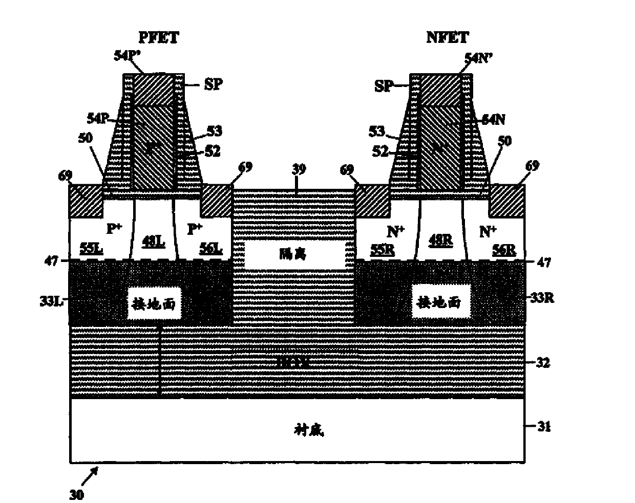
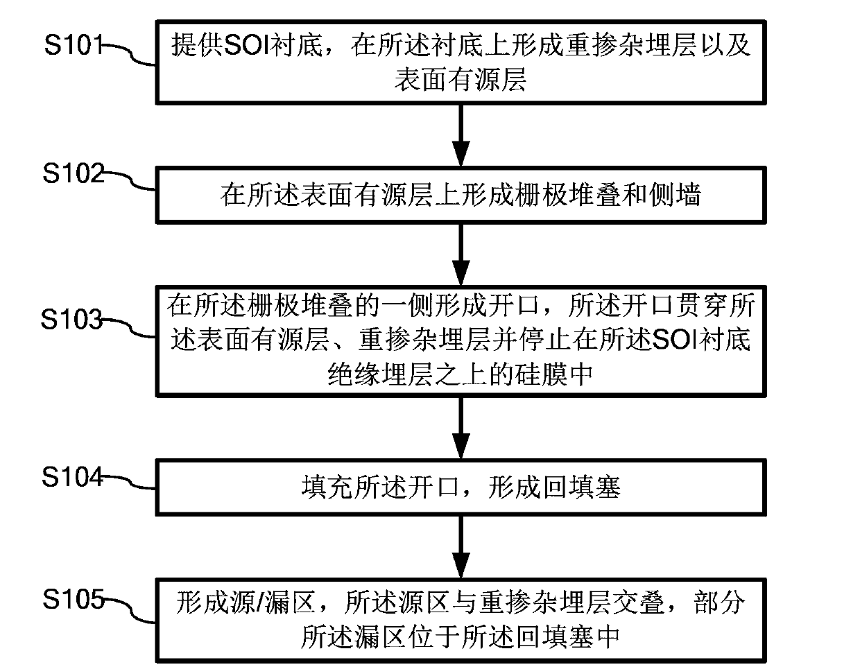
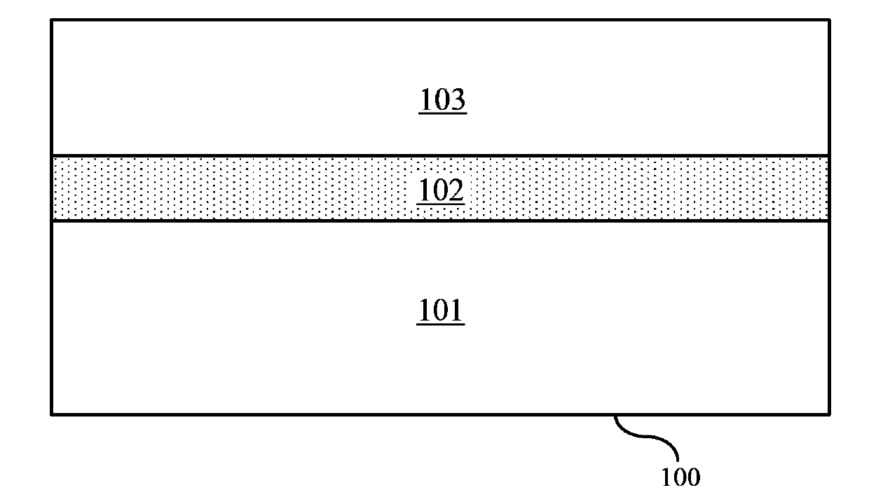
[0025] Embodiments of the present invention are described in detail below, examples of which are shown in the drawings, wherein the same or similar reference numerals designate the same or similar elements or elements having the same or similar functions throughout. The embodiments described below by referring to the figures are exemplary only for explaining the present invention and should not be construed as limiting the present invention. The following disclosure provides many different embodiments or examples for implementing different structures of the present invention. To simplify the disclosure of the present invention, components and arrangements of specific examples are described below. Of course, they are only examples and are not intended to limit the invention. Furthermore, the present invention may repeat reference numerals and / or letters in different instances. This repetition is for the purpose of simplicity and clarity and does not in itself indicate a relat...


PUM


Abstract

The invention provides a manufacturing method of a semiconductor structure. The method includes the steps of step 1, providing an SOI substrate and forming a heavy doping buried layer and a surface active layer on the substrate, step 2, forming a grid pile and a side wall on the substrate, step 3, forming an opening in one side of the grid pile, wherein the opening penetrates through the surface active layer and the heavy doping buried layer and stops in a silicon film above an insulation buried layer of the SOI substrate, step4, filling the opening to form a backfill plug, and step 5, forming a source region / drain region, wherein the source region and the heavy doping buried layer are overlapped, and partial drain region is placed in the backfill plug. Correspondingly, the invention further provides the semiconductor structure. According to the semiconductor structure and the manufacturing method thereof, the heavy doping buried layer is beneficial to reducing the width of a source region depletion layer / a drain region depletion layer and restricting the short-channel effect; the heavy doping buried layer and the source region are overlapped to form heavy doping pn junctions, therefore, the floating body effect of SOI MOS devices is effectively restricted, semiconductor device performance is effectively improved, leading out on regions is not needed, and the area and cost of devices are saved.

Description

technical field [0001] The invention relates to the field of semiconductor manufacturing, in particular to a semiconductor structure and a manufacturing method thereof. Background technique [0002] In order to improve the performance and integration of integrated circuit chips, the feature size of devices has been continuously reduced according to Moore's law, and has now entered the nanometer scale. As the size of devices shrinks, power consumption and leakage current become the most concerned issues. CMOS devices prepared by silicon on insulator SOI (Silicon on Insulator) have many advantages such as high speed, low power consumption, high integration, radiation resistance and no self-locking effect, and have become the preferred structure of deep submicron and nanoscale MOS devices. . SOI MOS devices are divided into two types according to the thickness of the silicon film and the maximum thickness of the surface depletion layer: partially depleted and fully depleted S...

Claims


Application Information

Patent Timeline
Patent Type & Authority Applications(China)
IPC IPC(8): H01L21/336H01L29/786H01L29/06
CPCH01L21/823807H01L21/84H01L29/78648H01L21/823814H01L29/66772H01L29/78612H01L27/1203H01L21/76283H01L21/02532H01L21/76264H01L29/6656H01L29/7841
Inventor 尹海洲朱慧珑骆志炯
Owner INST OF MICROELECTRONICS CHINESE ACAD OF SCI
Why Eureka
Try Eureka