MOS Structure with Suppressed SOI Floating Body Effect and Manufacturing Method thereof

a floating body effect and mos technology, applied in the direction of basic electric elements, electrical apparatus, semiconductor devices, etc., can solve the problems of low threshold voltage of fdsoi, high cost of thin film soi silicon, and inability to quickly transfer charge due to impact ionization mechanism, etc., to achieve the effect of not increasing the chip area

Inactive Publication Date: 2011-12-01
SHANGHAI INST OF MICROSYSTEM & INFORMATION TECH CHINESE ACAD OF SCI
View PDF36 Cites 2 Cited by
  • Summary
  • Abstract
  • Description
  • Claims
  • Application Information

AI Technical Summary

Benefits of technology

[0012]The feature of the present invention is that there is a highly doped P type region is under the source region. The highly doped P type region and highly doped N type region form a tunnel junction, so that the kink voltag...

Problems solved by technology

Thin film SOI silicon costs high and the threshold voltage of the FDSOI is hardly controlled.
The charge due to an impact ionization mechanism can not be transferred quickly, which will result in the...

Method used


Image

  • MOS Structure with Suppressed SOI Floating Body Effect and Manufacturing Method thereof
  • MOS Structure with Suppressed SOI Floating Body Effect and Manufacturing Method thereof
  • MOS Structure with Suppressed SOI Floating Body Effect and Manufacturing Method thereof

Examples


example i

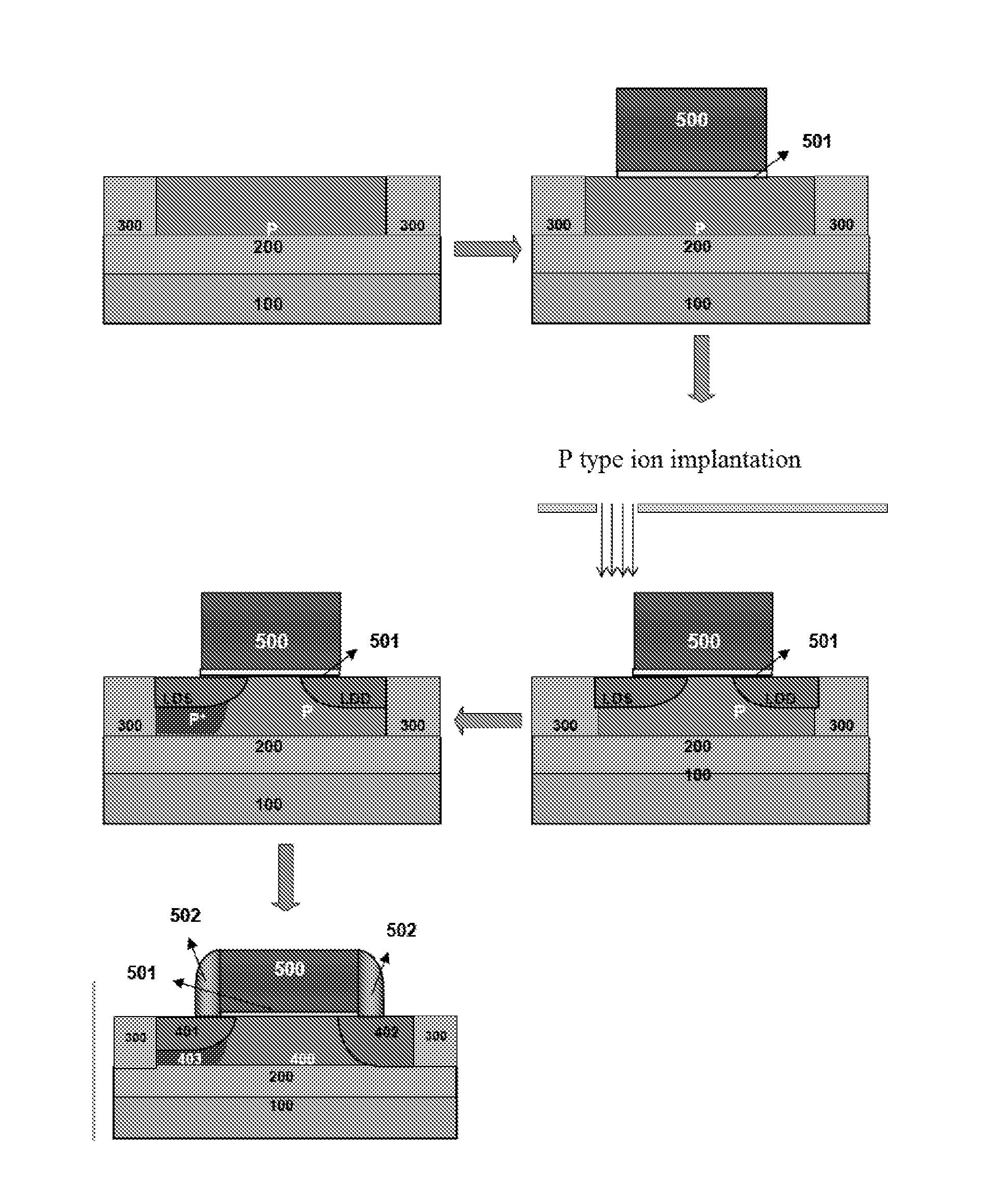
[0025]Referring to FIG. 3 of the drawings, this example provides a method of manufacturing MOS structure with suppressed floating body effect comprises the following steps.

[0026]Firstly, create a shallow trench isolation structure 300 on a semiconductor material, such as SOI (silicon on insulator) or GOI (germanium on insulator), having a buried insulation layer 200, to isolate an active area, and implant P ion into the active area. Add a mask on the active area, create an opening on the mask at a position of a first conductive type source region 401, and vertically highly implant P ions into the active area into via the mask forming a highly doped P region. Create a gate dielectric layer 501 and gate electrode 500. Lightly dope a source region and a drain region. Implant N ions into the source region and source region forming a first conductive type region 401 and a first conductive type drain region 402 and a body region 400 between the first conductive type region 401 and the fir...

example ii

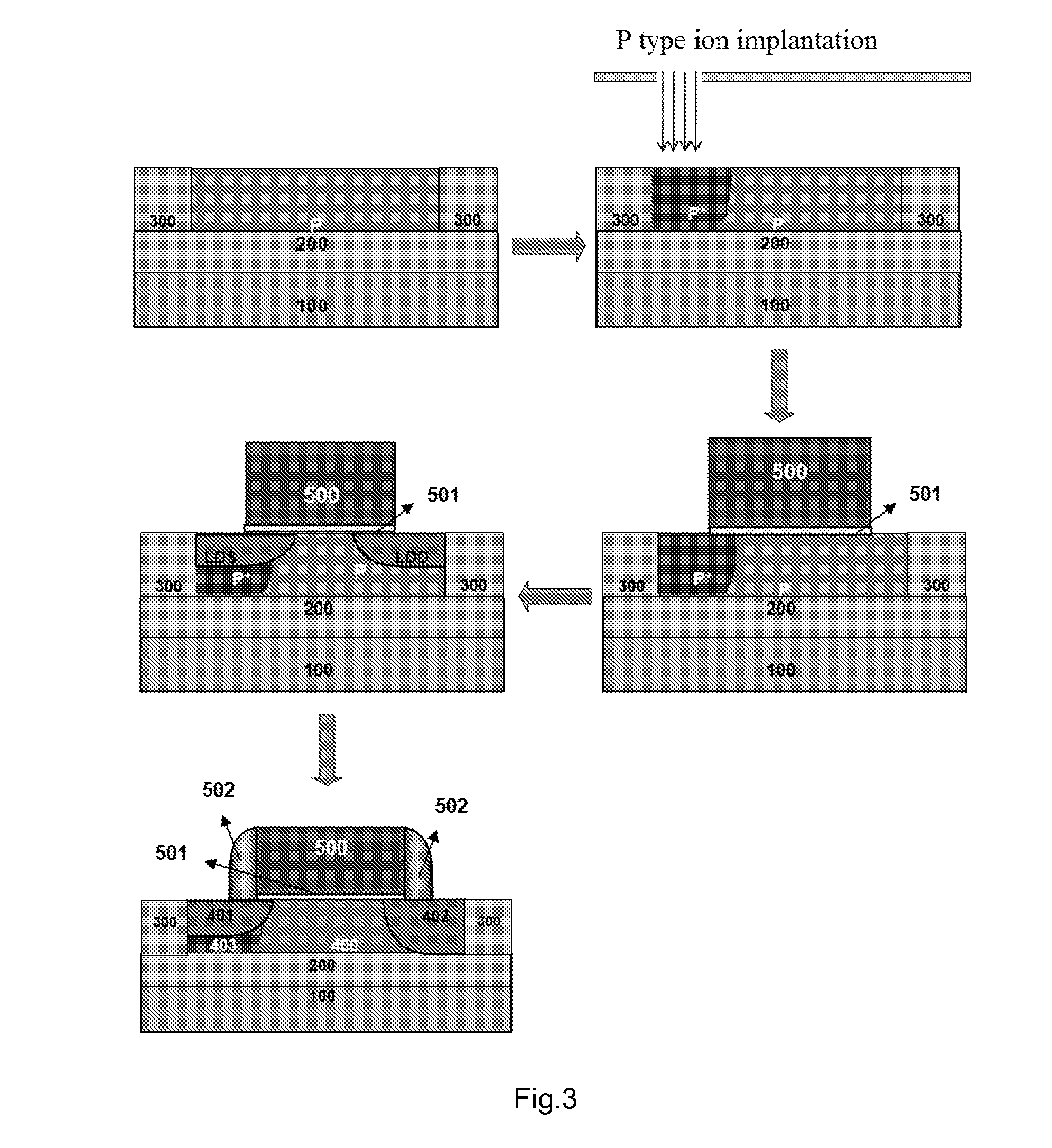
[0027]Referring to FIG. 4 of the drawings, this example provides a second method of manufacturing MOS structure with suppressed floating body effect comprises the following steps.

[0028]Firstly, create a shallow trench isolation structure 300 on a semiconductor material, such as SOI (silicon on insulator) or GOI (germanium on insulator), having a buried insulation layer 200, to isolate an active area, and implant P ion into the active area. Create a gate dielectric layer 501 and gate electrode 500. Lightly dope a source region and a drain region. Add a mask on the active area, create an opening on the mask at a position of a first conductive type source region 401, and vertically highly implant P ions into the active area into via the mask forming a highly doped P region under the lightly doped source region. Implant N ions into the source region and source region forming a first conductive type region 401 and a first conductive type drain region 402 and a body region 400 between the...

example iii

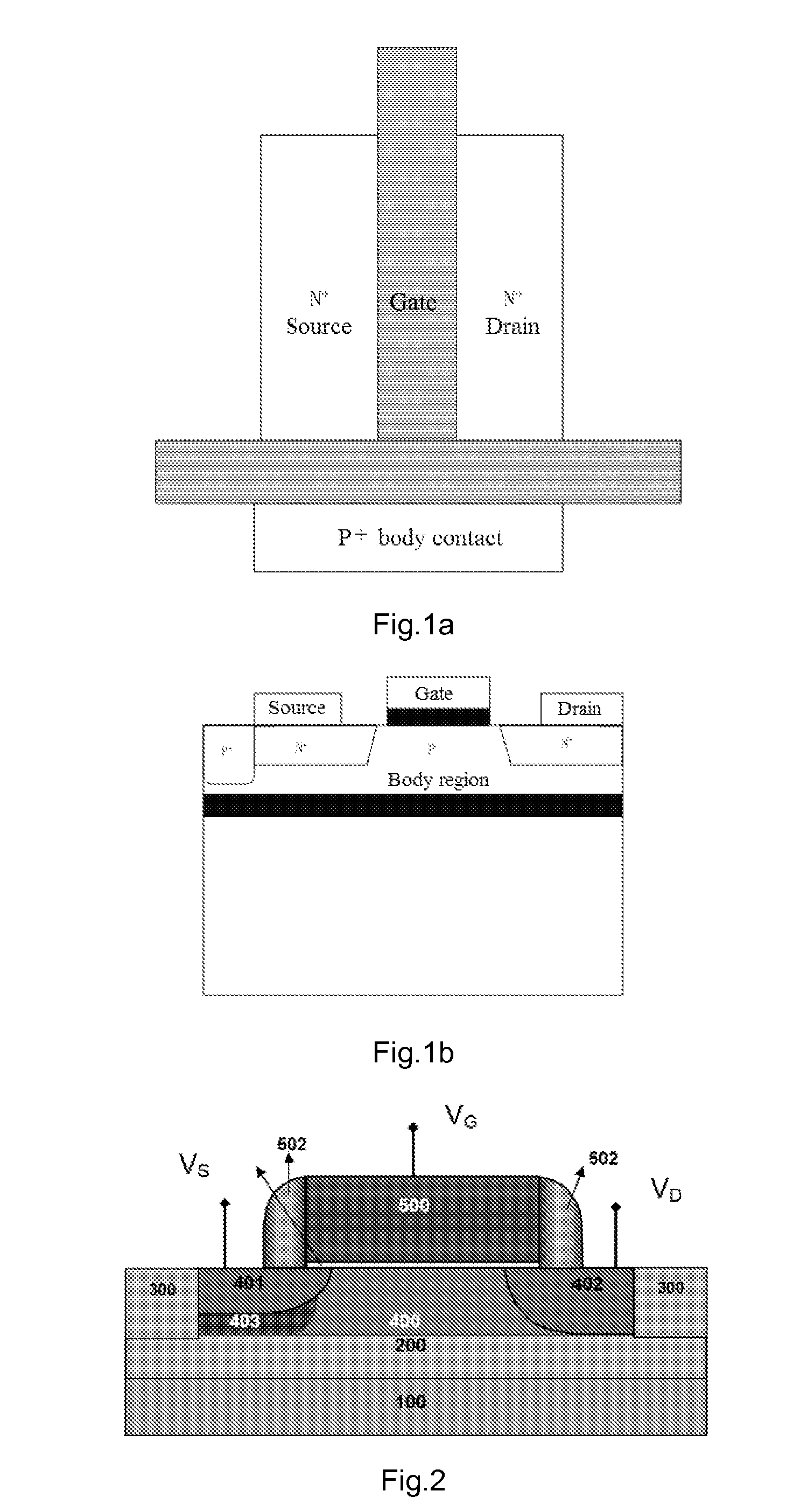
[0029]Referring to FIG. 5 of the drawings, this example provides a third method of manufacturing MOS structure with suppressed floating body effect comprises the following steps. Form a body region 400 on a semiconductor material, such as SOI (silicon on insulator) or GOI (germanium on insulator), having a buried insulation layer 200, a first conductive type source region 401 and a first conductive type drain region 402 provided on both sides of the body region 400 respectively, and a gate region on the body region 400 including a gate dielectric layer 501, a gate electrode 500 and an insulation dielectric spacer 502. Add a mask on the first conductive type source region 401, vertically highly implant P ions into the first conductive type source region 401 to form a high doped second conductive type region 403 under the first conductive type region 401 and on the buried insulation layer 200.

[0030]In order to analyze the performance of the MOS of the present invention, a simulation i...


PUM


Abstract

The present invention discloses a MOS structure with suppressed floating body effect including a substrate, a buried insulation layer provided on the substrate, and an active area provided on the buried insulation layer comprising a body region, a first conductive type source region and a first conductive type drain region provided on both sides of the body region respectively and a gate region provide on top of the body region, wherein the active area further comprises a highly doped second conductive type region between the first conductive type source region and the buried insulation layer. For manufacturing this structure, implant ions into a first conductive type source region via a mask having an opening thereon forming a highly doped second conductive type region under the first conductive type source region and above the buried insulation layer. The present invention will not increase chip area and is compatible with conventional CMOS process.

Description

BACKGROUND OF THE PRESENT INVENTION[0001]1. Field of Invention[0002]The present invention relates to a MOS (Metal Oxide Semiconductor) structure and a manufacturing method thereof, more particularly to a MOS structure with suppressed SOI floating body effect and manufacturing method thereof, which belongs to semiconductor manufacturing field.[0003]2. Description of Related Arts[0004]SOI means silicon on insulator. In SOI technique, device is fabricated in a very thin silicon film, and the device and substrate are separated by a buried oxide layer. This structure makes SOI have many advantages over bulk silicon technique. Small parasitic capacitance enable the high speed and low power consumption of the SOI device. Full dialectical isolation feature of SOI CMOS entirely eliminates the parasitic latch-up effect of bulk silicon CMOS device, and improve the integration density and the ability to resist radiation. SOI technique is widely used for RF, high voltage, and anti-radiation fiel...

Claims


Application Information

Patent Timeline
IPC IPC(8): H01L29/772
CPCH01L21/266H01L29/66772H01L29/1087H01L29/78624H01L29/78612
Inventor CHEN, JINGLUO, JIEXINWU, QINGQINGHUANG, XIAOLUWANG, XI
Owner SHANGHAI INST OF MICROSYSTEM & INFORMATION TECH CHINESE ACAD OF SCI
Why Eureka
Try Eureka