Semiconductor device

a technology of semiconductor devices and sub-layers, applied in semiconductor devices, semiconductor/solid-state device details, electrical apparatus, etc., can solve the problems of affecting the electric operation of the semiconductor device, affecting the reliability of the method to restrict the outflow range of the underfill, and the flow of the underfill overflowing from between the chip and the printed wiring board goes over the dam, so as to prevent an outflow

Active Publication Date: 2008-10-07
SHINKO ELECTRIC IND CO LTD
View PDF10 Cites 28 Cited by
  • Summary
  • Abstract
  • Description
  • Claims
  • Application Information

AI Technical Summary

Benefits of technology

[0015]The present invention has been made in view of the above circumstances, and provides a semiconductor device including a semiconductor chip, which is connected onto a surface of a printed wiring board in a flip-chip connection, and also including solder balls as external connection terminals for the semiconductor chip, wherein a flow of underfill is reliably prevented from overflowing outside by a dam corner portion being opposed to a corner portion of the semiconductor chip.
[0018]a dam for preventing an outflow of underfill, the dam being provided on the surface of the printed wiring board and surrounding an entire circumference of the semiconductor chip;

Problems solved by technology

Therefore, it is necessary to prevent the occurrence of such a problem that an overflowing underfill widely spreads and reaches a periphery portion, which negatively affects an electric operation of the semiconductor device.
However, both the chip connecting structures have a basic concept in common in which the outflow range of the resin is restricted by the dam.
Therefore, it is difficult for these methods to reliably restrict an outflow range of the underfill.
Accordingly, there is a high possibility that a flow of the underfill overflowing from between the chip and the printed wiring board goes over the dam and overflows outside.

Method used


Image

  • Semiconductor device
  • Semiconductor device
  • Semiconductor device

Examples


Embodiment Construction

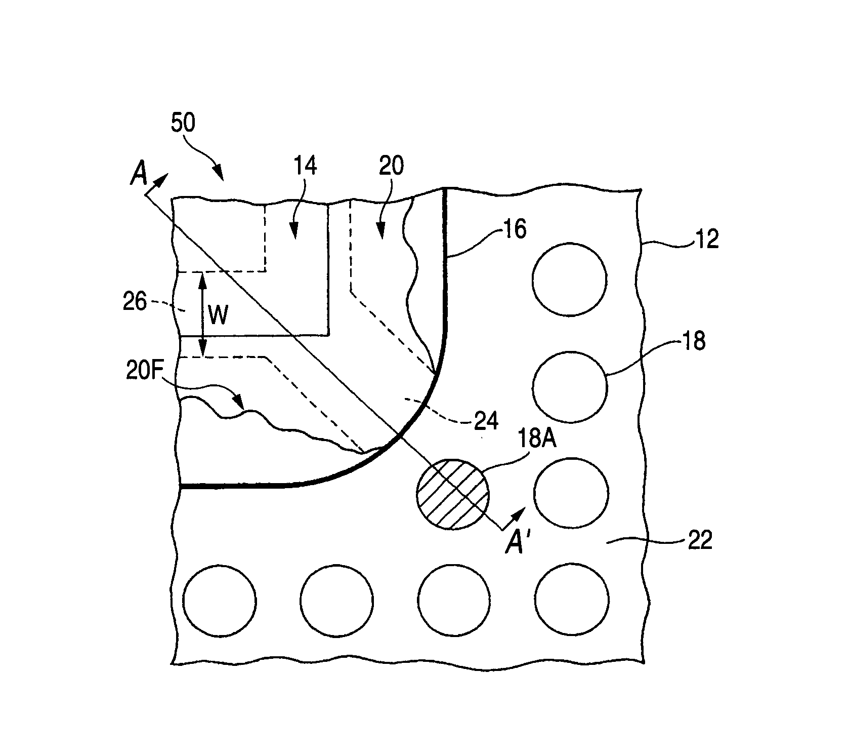
[0029]FIGS. 3A and 3B are views showing a portion of the semiconductor device of an embodiment of the present invention. FIG. 3A is a plan view showing a corner portion of a flip-chip connecting region, and FIG. 3B is a sectional view taken on line A-A′ in FIG. 3A.

[0030]In the semiconductor device 50 shown in the drawing, a semiconductor chip 14 is connected onto a surface of a printed wiring board 12 in a flip-chip connection.

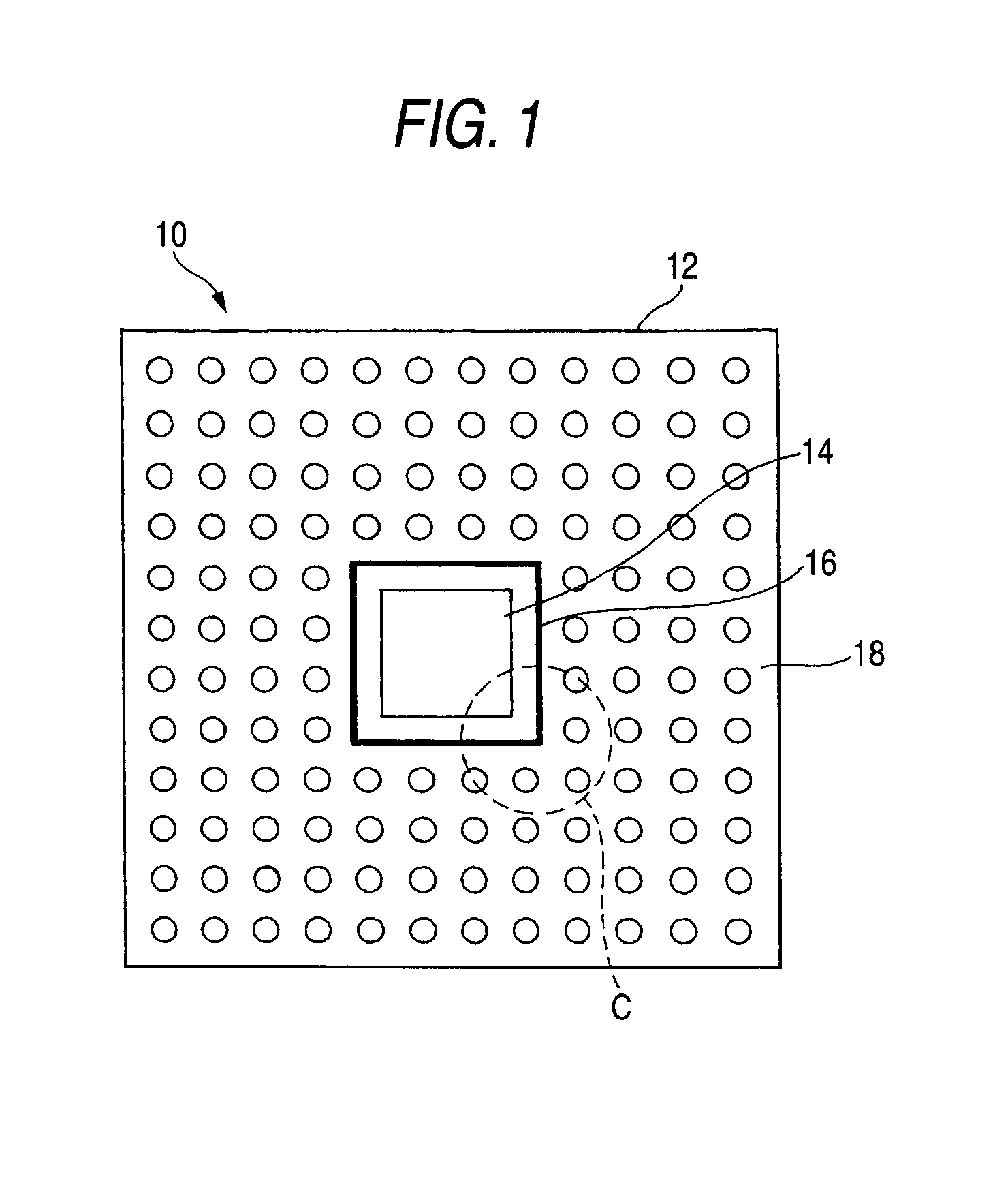
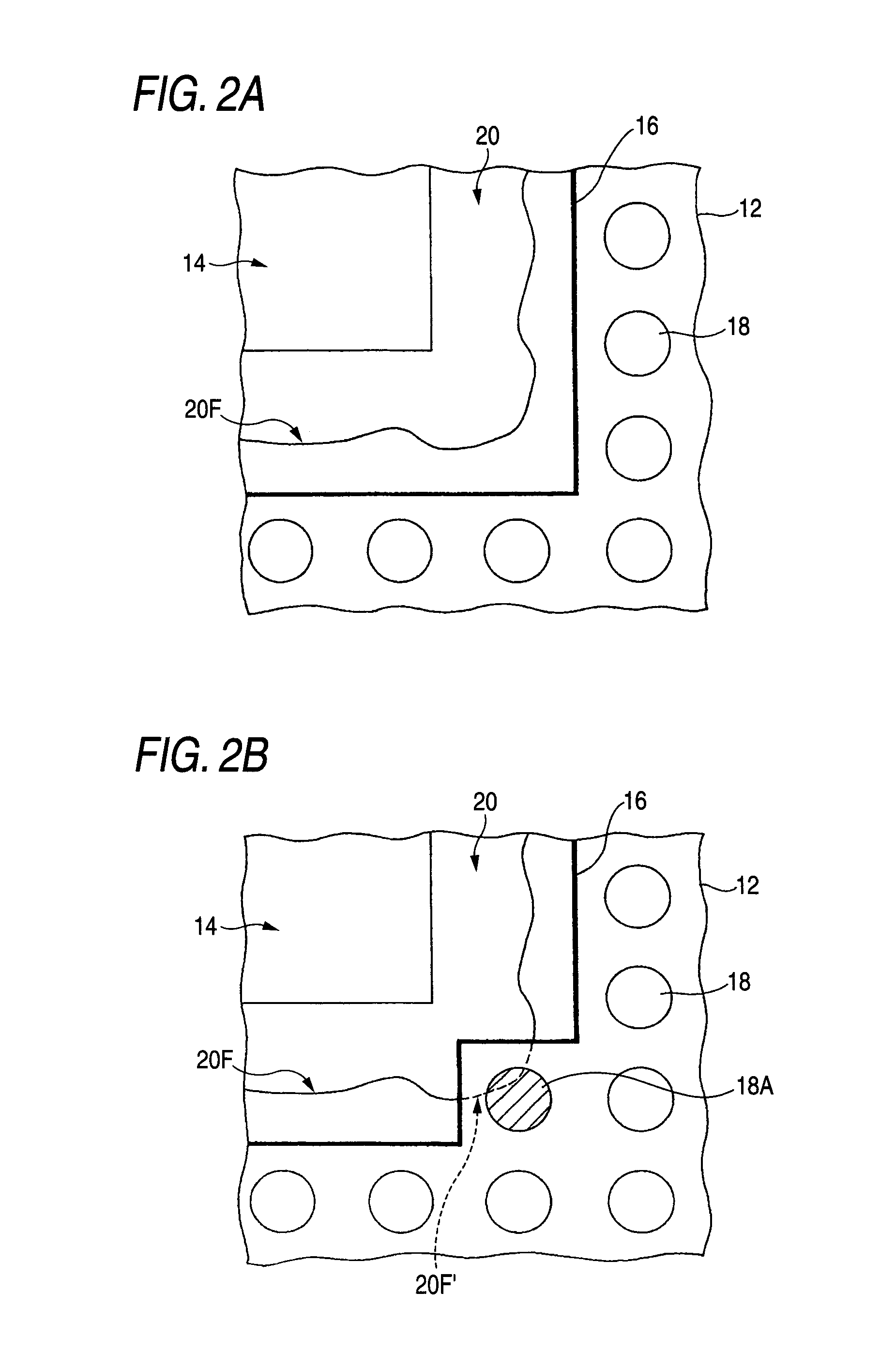
[0031]On the surface of the printed wiring board 12, a frame-shaped dam 16 for restricting an underfill outflow range surrounds an entire circumference of the semiconductor chip 14. Outside the frame-shaped dam 16, a solder ball 18A, which is used as an external connection terminal of the semiconductor chip 14, is arranged. The surface of the printed wiring board 12 except for flip-chip connecting portions and portions where solder balls are arranged is covered with a solder resist layer 22. The solder ball 18A is attached to a pad portion 23.

[0032]A recess po...


PUM


Abstract

A semiconductor device includes: a semiconductor chip connected onto a surface of a printed wiring board in a flip-chip connection; a dam for preventing an outflow of underfill, the dam being provided on the surface of the printed wiring board and surrounding an entire circumference of the semiconductor chip; an external connection terminal for the semiconductor chip, the external connection terminal being provided on the surface of the printed wiring board and arranged outside the dam; a solder resist layer covering the surface of the printed wiring board except for portions for the flip-chip connection and the external connection terminal arrangement; and at least one recess portion being provided in the solder resist layer and within a region between a corner portion of the semiconductor chip and a corner portion of the dam being opposed to the corner portion of the semiconductor chip.

Description

[0001]This application claims foreign priority based on Japanese Patent application No. 2005-242641, filed Aug. 24, 2005, the content of which is incorporated herein by reference in its entirety.BACKGROUND OF THE INVENTION[0002]1. Field of the Invention[0003]The present invention relates to a semiconductor device having a semiconductor chip being connected onto a surface of a printed wiring board in a flip-chip connection.[0004]2. Description of the Related Art[0005]In a structure in which a semiconductor chip is connected onto a printed wiring board in a flip-chip connection, in order to ensure the reliability of a connection of the chip with the printed wiring board, a gap formed between the chip and the board is filled with an underfill (sealing resin) so as to reinforce a connection of the chip with the printed wiring board. In order to enhance the reinforcing effect, the underfill is made to overflow a little from between the chip and the board to the periphery so that the over...

Claims


Application Information

Patent Timeline
Patent Type & Authority Patents(United States)
IPC IPC(8): H01L23/48H01L23/52H01L29/40
CPCH01L21/563H01L23/49816H01L2224/73203
Inventor KURAMOCHI, TOSHIYUKI
Owner SHINKO ELECTRIC IND CO LTD
Why Eureka
Try Eureka