Method of manufacturing semiconductor device including thin film transistor over thermal oxidation film over a glass substrate having distortion point of not lower than 750° C

a technology of thermal oxidation film and semiconductor device, which is applied in the direction of semiconductor devices, instruments, electrical equipment, etc., can solve the problems of increasing the cost of a product, increasing the cost of manufacturing, and high unit cost of the quartz substrate, and achieves high speed and high performan

Inactive Publication Date: 2005-05-10
SEMICON ENERGY LAB CO LTD
View PDF25 Cites 26 Cited by
  • Summary
  • Abstract
  • Description
  • Claims
  • Application Information

AI Technical Summary

Benefits of technology

[0019]The present invention has been made in order to satisfy the above requirements, and an object thereof is to realize a semiconductor de

Problems solved by technology

However, the quartz substrate has a high unit cost, so that the quartz substrate has problems of increasing the cost of manufacture, and further, increasing the cost of a product.
Thus, in recent years, attention has been paid to a low temperature polysilicon film formed on an inexpensive glass substrate, and the research of the high temperature polysilicon film has been gradually declined.
Moreover, since it is difficult to make the quartz substrate large, the use of a TFT using the high temperature polysilicon is limited to a liquid crystal display device with a size of about 1 to 2 inches in diagonal for a projection type projector or the like.
That is, there is a problem th

Method used


Image

  • Method of manufacturing semiconductor device including thin film transistor over thermal oxidation film over a glass substrate having distortion point of not lower than 750° C
  • Method of manufacturing semiconductor device including thin film transistor over thermal oxidation film over a glass substrate having distortion point of not lower than 750° C
  • Method of manufacturing semiconductor device including thin film transistor over thermal oxidation film over a glass substrate having distortion point of not lower than 750° C

Examples


embodiment 1

[0192]In this embodiment, manufacturing steps of a semiconductor device having the structure of the present invention will be described with reference to FIGS. 4A to 4D. Specifically, there is shown an example in which a driving circuit constituted by CMOS circuits in which an NTFT (N-channel TFT) and a PTFT (P-channel TFT) using a polysilicon film are complementarily combined, and a pixel matrix circuit constituted by NTFTs are integrally formed on the same substrate.

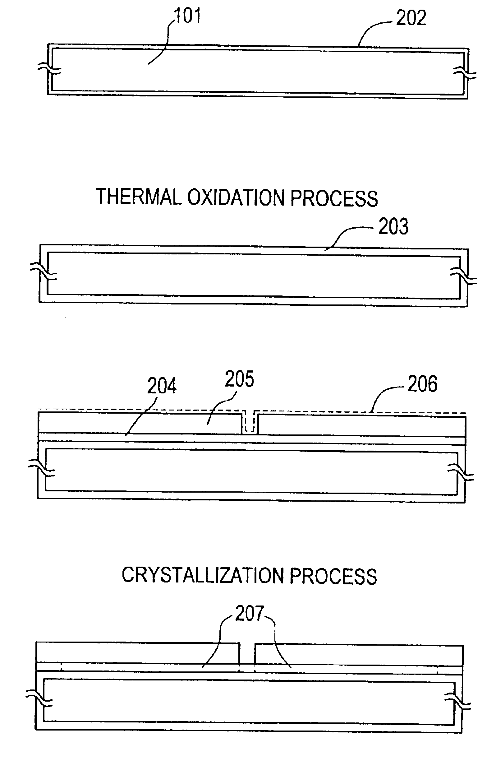
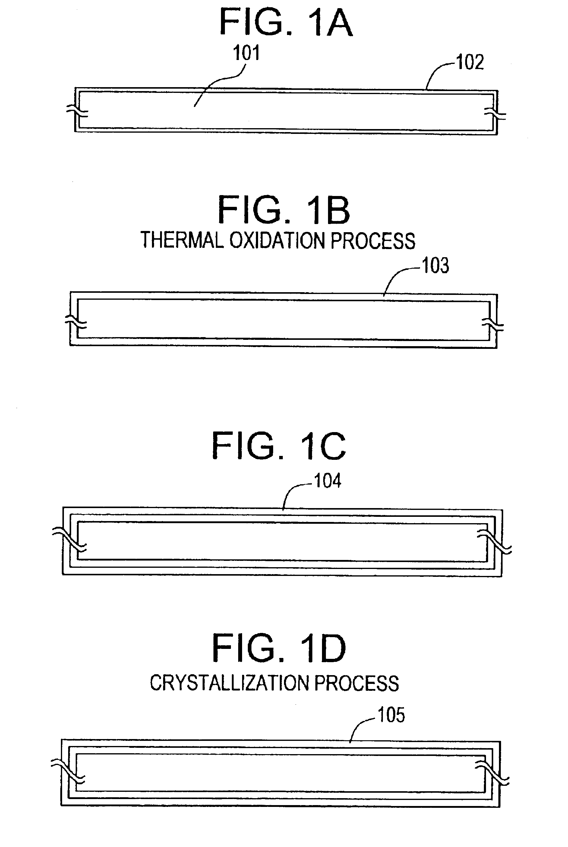
[0193]First, in accordance with the manufacturing steps explained by using FIGS. 1A to 1D, a crystalline silicon film (typically, polycrystal silicon film) 105 is formed. Then the polycrystal silicon film 105 is patterned to form active layers 403 to 405. At this time, although the polycrystal silicon film formed on the side surface of a crystallized glass 401 is removed, the polycrystal silicon film on the back surface remains as it is.

[0194]Reference numeral 403 denotes the active layer of the PTFT of the CMOS circui...

embodiment 2

[0218]In this embodiment, manufacturing steps of a semiconductor device having the structure of the present invention will be described with reference to FIGS. 6A to 6D. Specifically, there is shown an example in which a driving circuit and a logic circuit constituted by CMOS circuits in which an NTFT (N-channel TFT) and a PTFT (P-channel TFT) using CGS are complementarily combined, and a pixel matrix circuit constituted by NTFTs are integrally formed on the same substrate.

[0219]The logic circuit is a signal processing circuit having functions different from those of a driving circuit typified by a shift register or the like, and is a general term of a circuit for performing such signal processing as is conventionally carried out by an external IC, such as a D / A converter circuit, a memory circuit, a γ correction circuit, a calculation processing circuit, and the like.

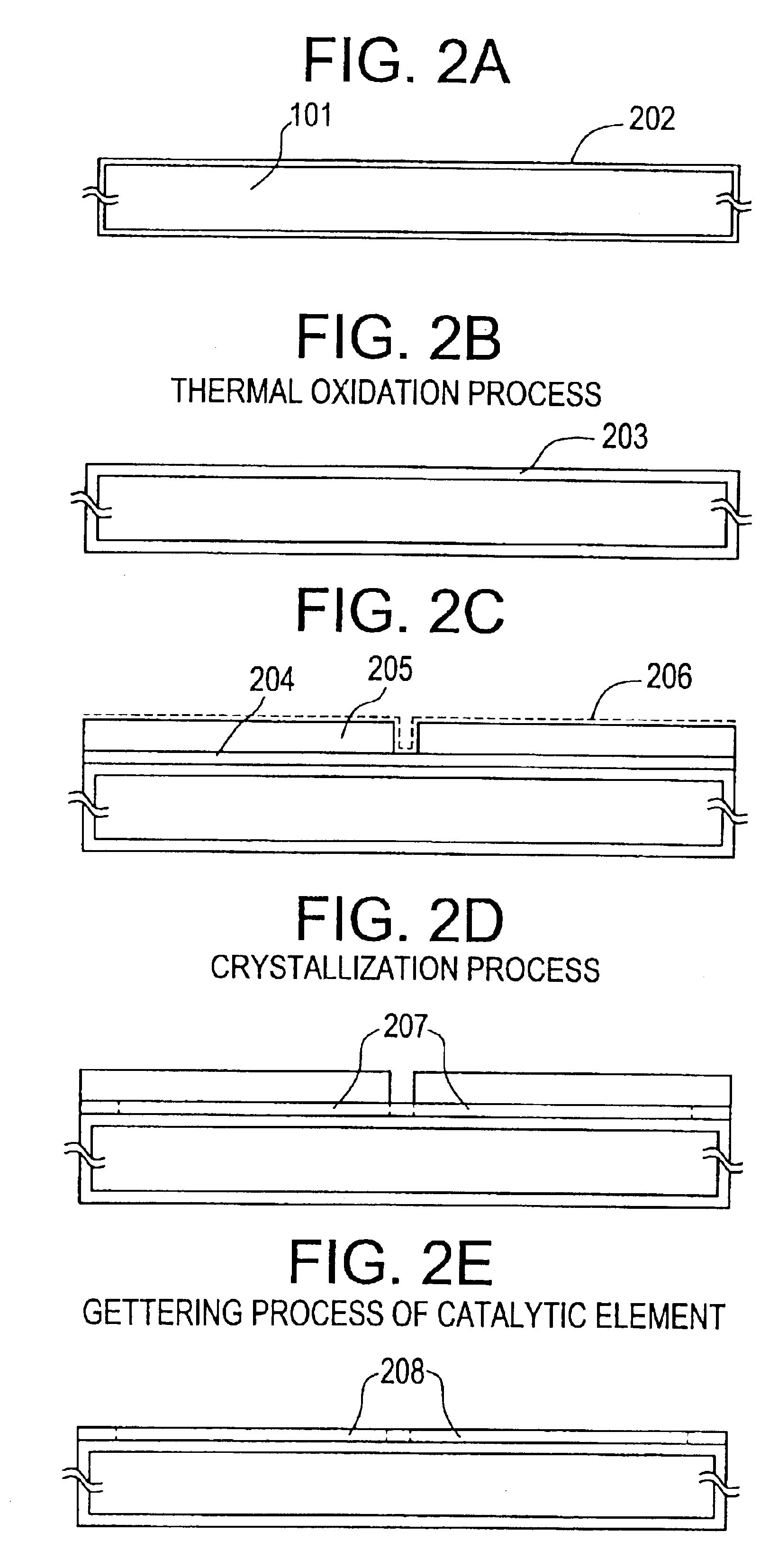
[0220]First, in accordance with the manufacturing steps explained by using FIGS. 2A to 2E, steps up to the gettering...

embodiment 3

[0247]In this embodiment, an example in which an insulating silicon film for protecting crystallized glass in the structure of Embodiment 1 is formed by a low pressure CVD method, will be described.

[0248]First, as a substrate, crystallized glass having the composition of SiO2: 52.5, Al2O3: 26.5, MgO: 11.9, TiO2: 11.4 is prepared. This is non-alkaline cordierite-based crystallized glass using TiO2 as a nucleus forming agent.

[0249]Next, a silicon nitride oxide film is formed on the front surface, the back surface, and the side surface of the crystallized glass. In this embodiment, the silicon nitride oxide film is formed by a low pressure CVD method using silane (SiH4) and nitrous oxide (N2O) as a film forming gas.

[0250]In this case, a film forming temperature is 800 to 850° C. (in this embodiment, 850° C.), and the flow rates of the respective film forming gases are made SiH4: 10 to 30 sccm and N2O: 300 to 900 sccm. It is appropriate that the reaction pressure is made 0.5 to 1.0 torr...


PUM


Abstract

When a crystalline semiconductor thin film formed by using a catalytic element for facilitating crystallization is subjected to a heat treatment in an atmosphere containing a halogen element at a temperature exceeding 700° C., a crystal structure in which crystal grain boundaries do not substantially exist can be obtained. In the present invention, the foregoing crystalline semiconductor thin film is formed on a crystallized glass substrate which is inexpensive and has high heat resistance, so that an inexpensive semiconductor device can be provided.

Description

BACKGROUND OF THE INVENTION[0001]1. Field of the Invention[0002]The present invention relates to a semiconductor device using a crystalline semiconductor thin film formed on a substrate having an insulating surface.[0003]Incidentally, in the present specification, any of a thin film transistor (hereinafter referred to as a TFT), a semiconductor circuit, an electrooptical device, and an electronic equipment are included in the category of the semiconductor device. That is, any device capable of functioning by using semiconductor characteristics will be referred to as the semiconductor device.[0004]Thus, the semiconductor device recited in claims of the present application includes not only a single component, such as a thin film transistor, but also a semiconductor circuit or an electrooptical device formed by integrating such single components, and further, an electronic equipment having those as parts.[0005]2. Description of the Related Art[0006]In recent years, attention has been ...

Claims


Application Information

Patent Timeline
IPC IPC(8): H01L21/02H01L21/70H01L29/66H01L21/336H01L27/12H01L29/786H01L21/84G02F1/13G02F1/1362G02F1/1333H01L21/77H01L29/04
CPCH01L27/12H01L29/04H01L29/045H01L27/1277H01L29/78603H01L29/78675H01L29/78678H01L27/1248H01L29/66757G02F1/13454G02F2001/133302G02F1/133302H01L21/18
Inventor YAMAZAKI, SHUNPEIOHTANI, HISASHI
Owner SEMICON ENERGY LAB CO LTD
Why Eureka
Try Eureka