Semiconductor device

Active Publication Date: 2007-03-01
SHINKO ELECTRIC IND CO LTD
View PDF7 Cites 22 Cited by
  • Summary
  • Abstract
  • Description
  • Claims
  • Application Information

AI Technical Summary

Benefits of technology

[0015] The present invention has been made in view of the above circumstances, and provides a semiconductor device including a semiconductor chip, which is connected onto a surface of a printed wiring board in a flip-chip connection, and also

Problems solved by technology

Therefore, it is necessary to prevent the occurrence of such a problem that an overflowing underfill widely spreads and reaches a periphery portion, which negatively affects an electric operation of the semiconductor device.
However, both the chip connecting structures have a basic concept in common in which the outflo

Method used


Image

  • Semiconductor device
  • Semiconductor device
  • Semiconductor device

Examples


Embodiment Construction

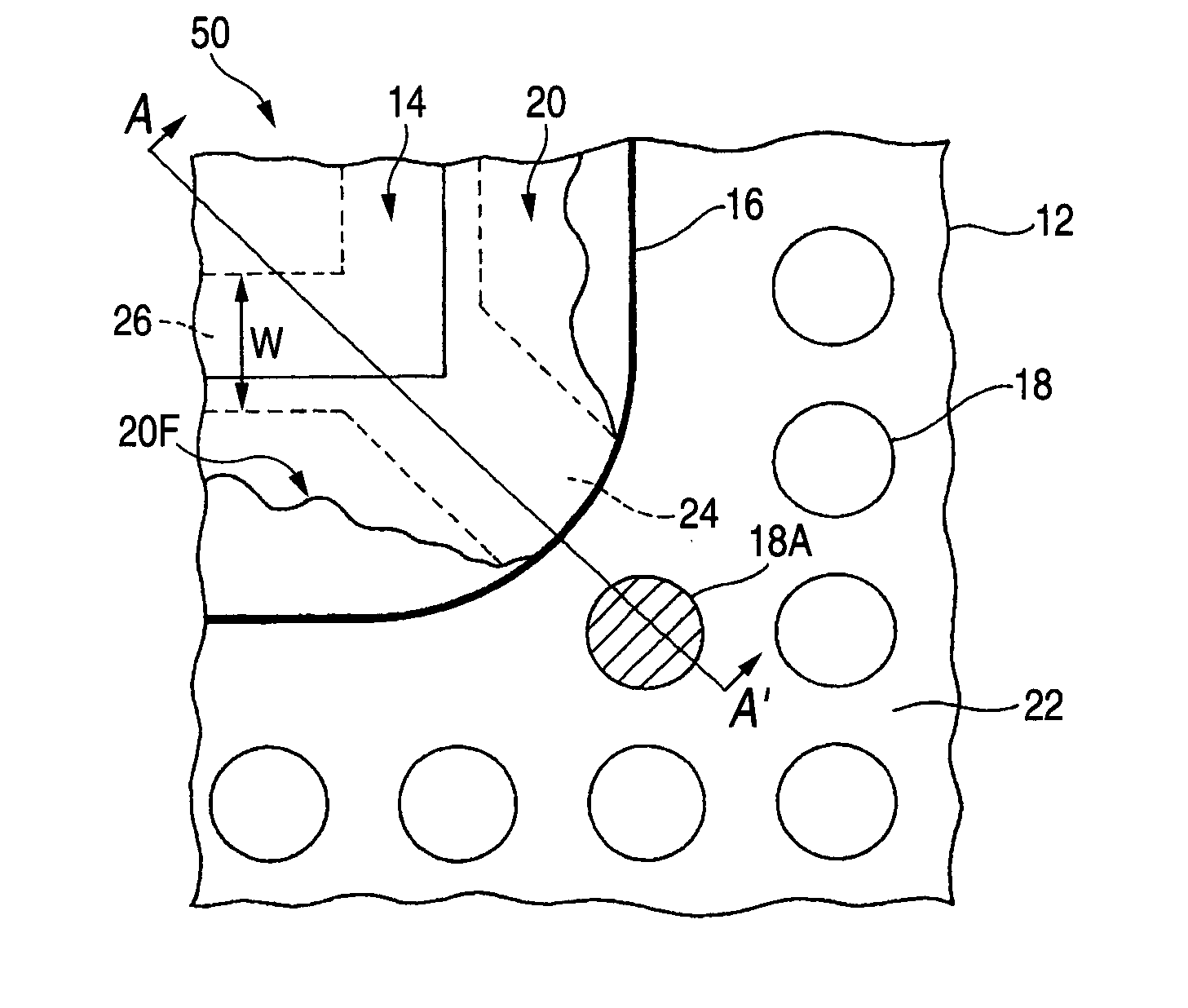
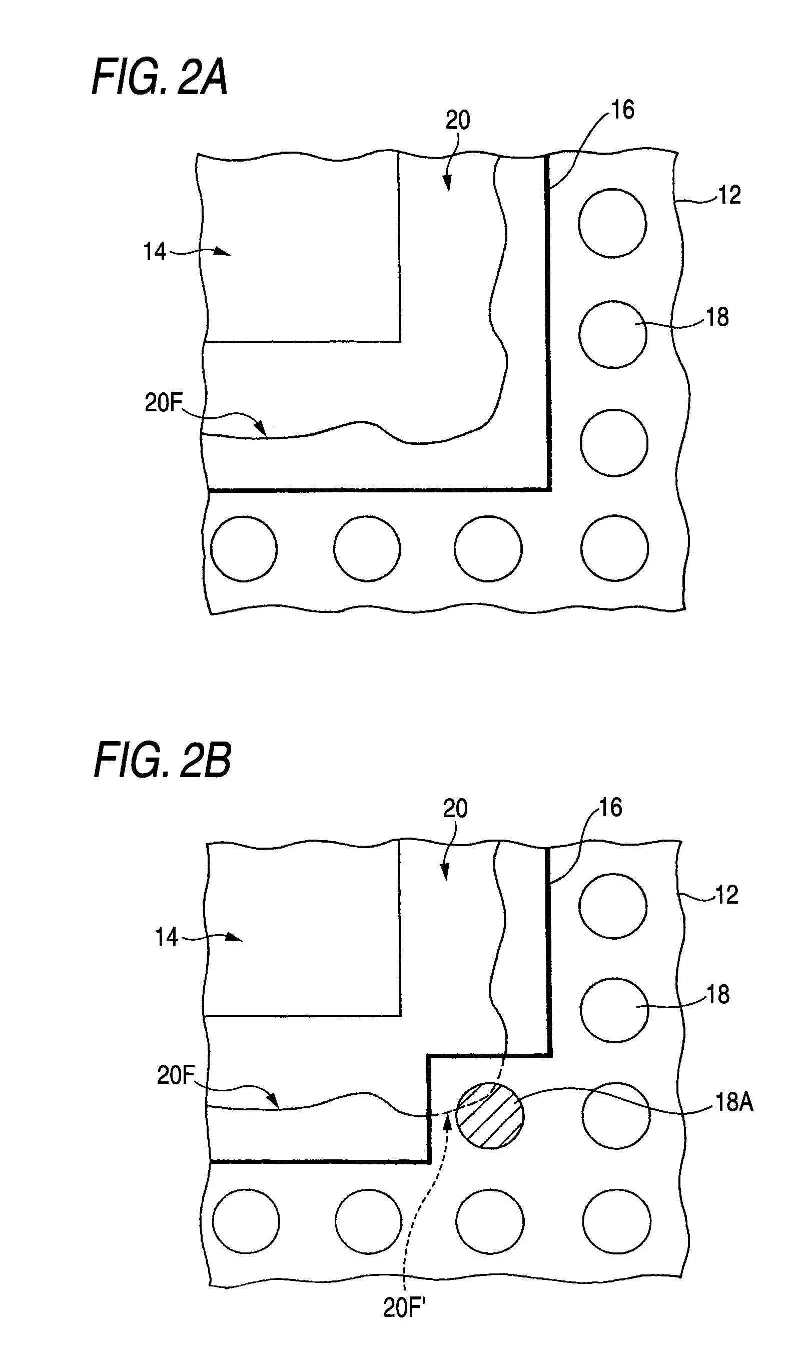
[0029]FIGS. 3A and 3B are views showing a portion of the semiconductor device of an embodiment of the present invention. FIG. 3A is a plan view showing a corner portion of a flip-chip connecting region, and FIG. 3B is a sectional view taken on line A-A′ in FIG. 3A.

[0030] In the semiconductor device 50 shown in the drawing, a semiconductor chip 14 is connected onto a surface of a printed wiring board 12 in a flip-chip connection.

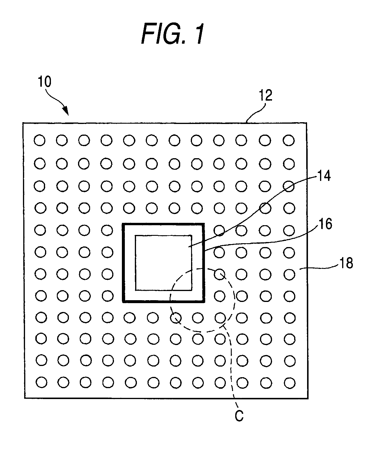
[0031] On the surface of the printed wiring board 12, a frame-shaped dam 16 for restricting an underfill outflow range surrounds an entire circumference of the semiconductor chip 14. Outside the frame-shaped dam 16, a solder ball 18A, which is used as an external connection terminal of the semiconductor chip 14, is arranged. The surface of the printed wiring board 12 except for flip-chip connecting portions and portions where solder balls are arranged is covered with a solder resist layer 22. The solder ball 18A is attached to a pad portion 23.

[0032] A rec...


PUM


Abstract

A semiconductor device includes: a semiconductor chip connected onto a surface of a printed wiring board in a flip-chip connection; a dam for preventing an outflow of underfill, the dam being provided on the surface of the printed wiring board and surrounding an entire circumference of the semiconductor chip; an external connection terminal for the semiconductor chip, the external connection terminal being provided on the surface of the printed wiring board and arranged outside the dam; a solder resist layer covering the surface of the printed wiring board except for portions for the flip-chip connection and the external connection terminal arrangement; and at least one recess portion being provided in the solder resist layer and within a region between a corner portion of the semiconductor chip and a corner portion of the dam being opposed to the corner portion of the semiconductor chip.

Description

[0001] This application claims foreign priority based on Japanese Patent application No. 2005-242641, filed Aug. 24, 2005, the content of which is incorporated herein by reference in its entirety. BACKGROUND OF THE INVENTION [0002] 1. Field of the Invention [0003] The present invention relates to a semiconductor device having a semiconductor chip being connected onto a surface of a printed wiring board in a flip-chip connection. [0004] 2. Description of the Related Art [0005] In a structure in which a semiconductor chip is connected onto a printed wiring board in a flip-chip connection, in order to ensure the reliability of a connection of the chip with the printed wiring board, a gap formed between the chip and the board is filled with an underfill (sealing resin) so as to reinforce a connection of the chip with the printed wiring board. In order to enhance the reinforcing effect, the underfill is made to overflow a little from between the chip and the board to the periphery so tha...

Claims


Application Information

Patent Timeline
IPC IPC(8): H01L23/48
CPCH01L21/563H01L2224/73203H01L23/49816
Inventor KURAMOCHI, TOSHIYUKI
Owner SHINKO ELECTRIC IND CO LTD
Why Eureka
Try Eureka