Polish stop and sealing layer for manufacture of semiconductor devices with deep trench isolation

a technology of trench isolation and sealing layer, which is applied in the direction of semiconductor/solid-state device manufacturing, basic electric elements, electric apparatus, etc., can solve the problems of increasing the difficulty of excluding inter-element interference, low-cost dielectric films typically have less desirable electrical characteristics, and achieve the effect of eliminating or drastically reducing the possibility of polysilicon stringers

Active Publication Date: 2008-10-14
ATMEL CORP
View PDF11 Cites 54 Cited by
  • Summary
  • Abstract
  • Description
  • Claims
  • Application Information

AI Technical Summary

Benefits of technology

[0008]The present invention is a method and resulting device that eliminates vertical steps or gaps in a deep trench isolation region and, thus, eliminates or drastically reduces a possibility of polysilicon stringers. Additionally, the invention allows an inexpensive dielectric material, for example a lower-quality silicon dioxide to be used to fill the deep trench and a higher quality oxide, in an electrically active region, to be used on an uppermost portion of the deep trench without either affecting device performance or increasing a possibility of forming polysilicon stringers.
[0010]Notice that the third and fourth silicon dioxide layers may be different types of oxide with third oxide (i.e., the deep trench fill oxide) being of a lower quality than the fourth silicon dioxide layer (i.e., the layer in closest proximity to an active device region). Overall fabrication costs are thereby reduced without sacrificing the electrical performance of the active device. A region of the second silicon nitride layer overlaying the first silicon dioxide layer and the first silicon nitride layer prevents any gaps or vertical steps from forming.

Problems solved by technology

However, as the degree to which semiconductor devices are integrated continues to increase and a size of the various elements is minimized to reduce a distance between the elements or increase a density of the elements, it becomes increasingly difficult to exclude inter-element interference.
Low-cost dielectric films typically have less desirable electrical characteristics (e.g., dielectric breakdown strength or higher shrinkage values) than a high-quality film.
However, due to their increased cost (either in terms of material used for their production and / or processing techniques required for their formation and deposition), high-quality films are unsuitable for filling the deep trench.
Overetching the polysilicon film to eliminate stringers is undesirable since (1) increased costs result from added or prolonged fabrication steps or operations; and (2) required conductive features may also be etched away.
The electrical shorts can produce catastrophic failures in one or more active devices on an integrated circuit (IC) chip, consequently leading to low fabrication yield.

Method used


Image

  • Polish stop and sealing layer for manufacture of semiconductor devices with deep trench isolation
  • Polish stop and sealing layer for manufacture of semiconductor devices with deep trench isolation
  • Polish stop and sealing layer for manufacture of semiconductor devices with deep trench isolation

Examples


Embodiment Construction

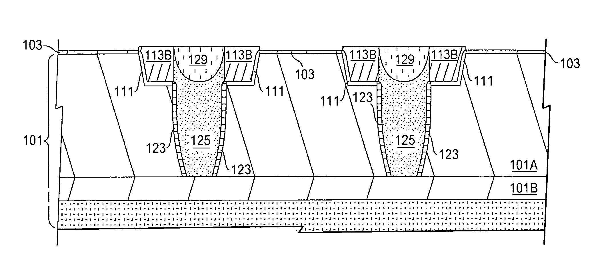
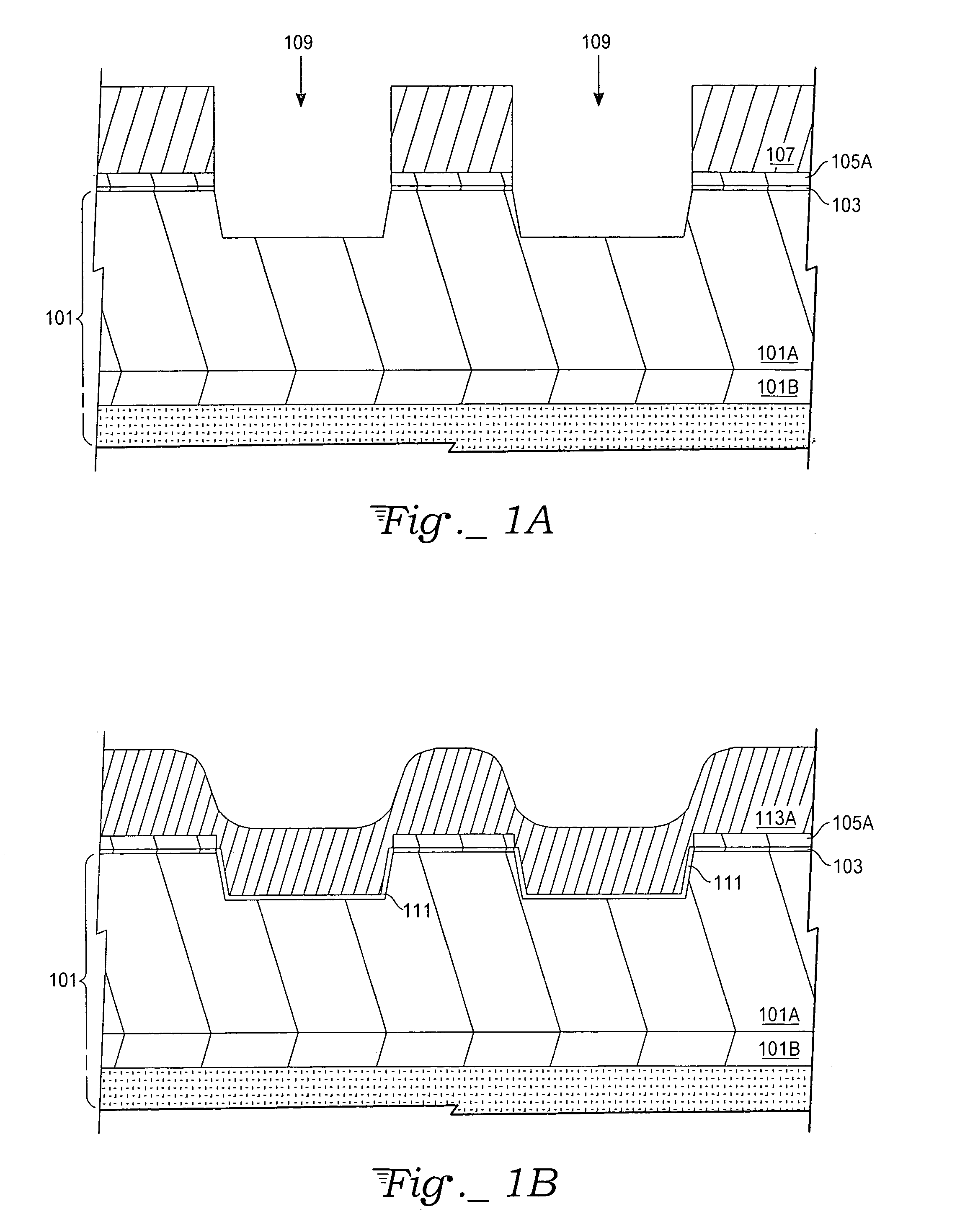
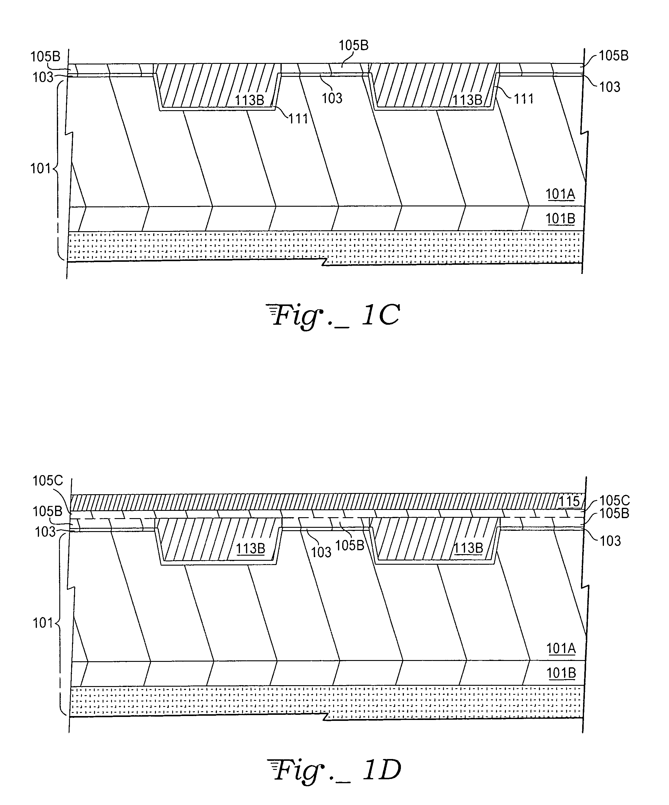
[0014]With reference to FIG. 1A, early exemplary fabrication steps of a deep trench isolation structure begin with a base substrate 101. In a specific exemplary embodiment, the base substrate 101 is a C-flat, silicon on insulator (SOI) over silicon substrate. In the specific exemplary embodiment, the silicon cap layer 101A is approximately 2 μm (2000 nm) in thickness and is bonded to an SOI insulator layer 101B. In other embodiments, the base substrate 101 may be a silicon wafer. Alternatively, another elemental group IV semiconductor or compound semiconductor (e.g., group III-V) may be selected for the base substrate 101. In a case where the base substrate 101 is a semiconductor wafer, the wafer may contain a buried oxide layer (not shown) placed below a polysilicon layer (not shown) to prevent transport of carriers through the underlying bulk semiconducting material. The polysilicon is then treated at an elevated temperature to reform crystalline (i.e., non-amorphous) silicon. In ...


PUM


Abstract

A method and resulting device that eliminates vertical steps or gaps in a deep trench isolation region and, thus, eliminates or drastically reduces a possibility of polysilicon stringers. Additionally, the invention allows an inexpensive dielectric material, for example a lower-quality silicon dioxide to be used to fill the deep trench and a higher quality oxide, in an electrically active region, to be used on an uppermost portion of the deep trench without affecting device performance or increasing a possibility of forming polysilicon stringers.

Description

TECHNICAL FIELD[0001]The present invention relates to semiconductor processing. More specifically, the invention is a fabrication method for deep trench isolation and a resulting integrated circuit structure.BACKGROUND ART[0002]To form a semiconductor device, a multitude of elements are formed on or near a surface layer of a semiconductor substrate and electrically connected with each other through conductive lines. Accordingly, there is need for each element formed in a narrow region on the substrate to be electrically isolated from adjacent elements such that the elements are not electrically influenced by each other. For this, in the semiconductor device, an isolation layer or isolation structure is commonly used.[0003]However, as the degree to which semiconductor devices are integrated continues to increase and a size of the various elements is minimized to reduce a distance between the elements or increase a density of the elements, it becomes increasingly difficult to exclude ...

Claims


Application Information

Patent Timeline
Patent Type & Authority Patents(United States)
IPC IPC(8): H01L21/473
CPCH01L21/763
Inventor MILLER, GAYLEBROWN, ERIC
Owner ATMEL CORP
Why Eureka
Try Eureka