Power source circuit

a power source circuit and circuit technology, applied in the direction of power conversion systems, instruments, dc-dc conversion, etc., can solve the problems of increasing ripple in the output increasing the write-enable write potential of the cell, and increasing the ripple of the boosting circuit output, so as to reduce the voltage dividing ratio

Active Publication Date: 2008-10-21
KIOXIA CORP
View PDF9 Cites 23 Cited by
  • Summary
  • Abstract
  • Description
  • Claims
  • Application Information

AI Technical Summary

Problems solved by technology

When the resistance value of the voltage dividing resistors is large, when the operation delay of the comparison amplifier is large, and when the boosting capability of the boosting circuit is large, the ripple is increased.
However, the cell characteristics are not uniform for all the cells, which causes the write-enable write potential for the cell to be different.
Thus, as described above, in the case where the set potential is changed, there is a problem that when the set potential is low, the ripple in the output of the boosting circuit is increased.
However, as described above, in the writing operation to the cells having a low write-enable potential, when the output of the boosting circuit is set to low by adjusting the voltage dividing resistance of the power source detecting circuit, the ripple is increased in the conventional circuit, so that the writing characteristic to the memory cell is deteriorated.
Therefore, in the above described conventional technique, it is not possible to reduce the set potential dependency of the boosting capability and to reduce the ripple, in correspondence with a plurality of set potentials.

Method used


Image

  • Power source circuit
  • Power source circuit
  • Power source circuit

Examples


embodiment

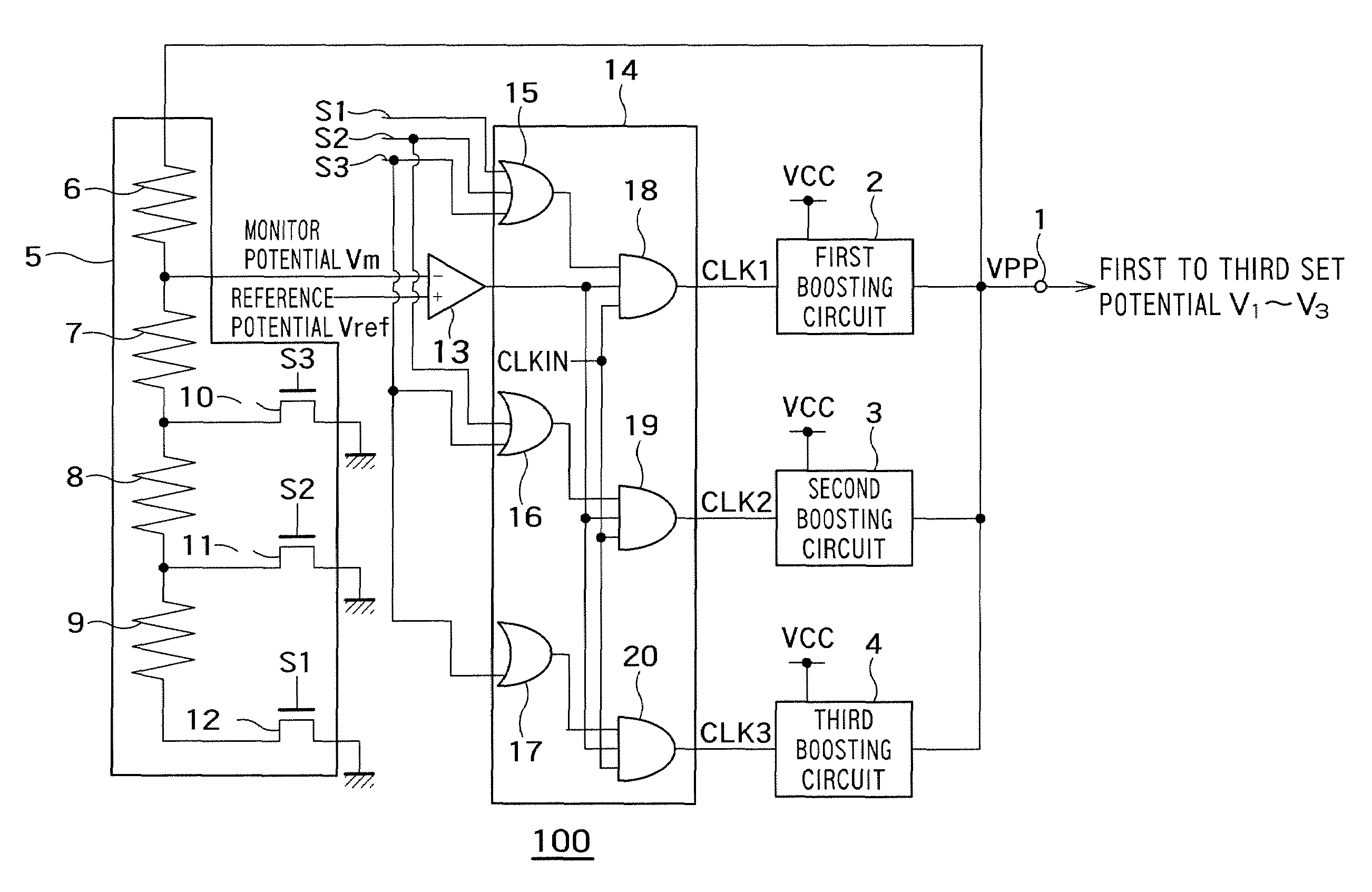
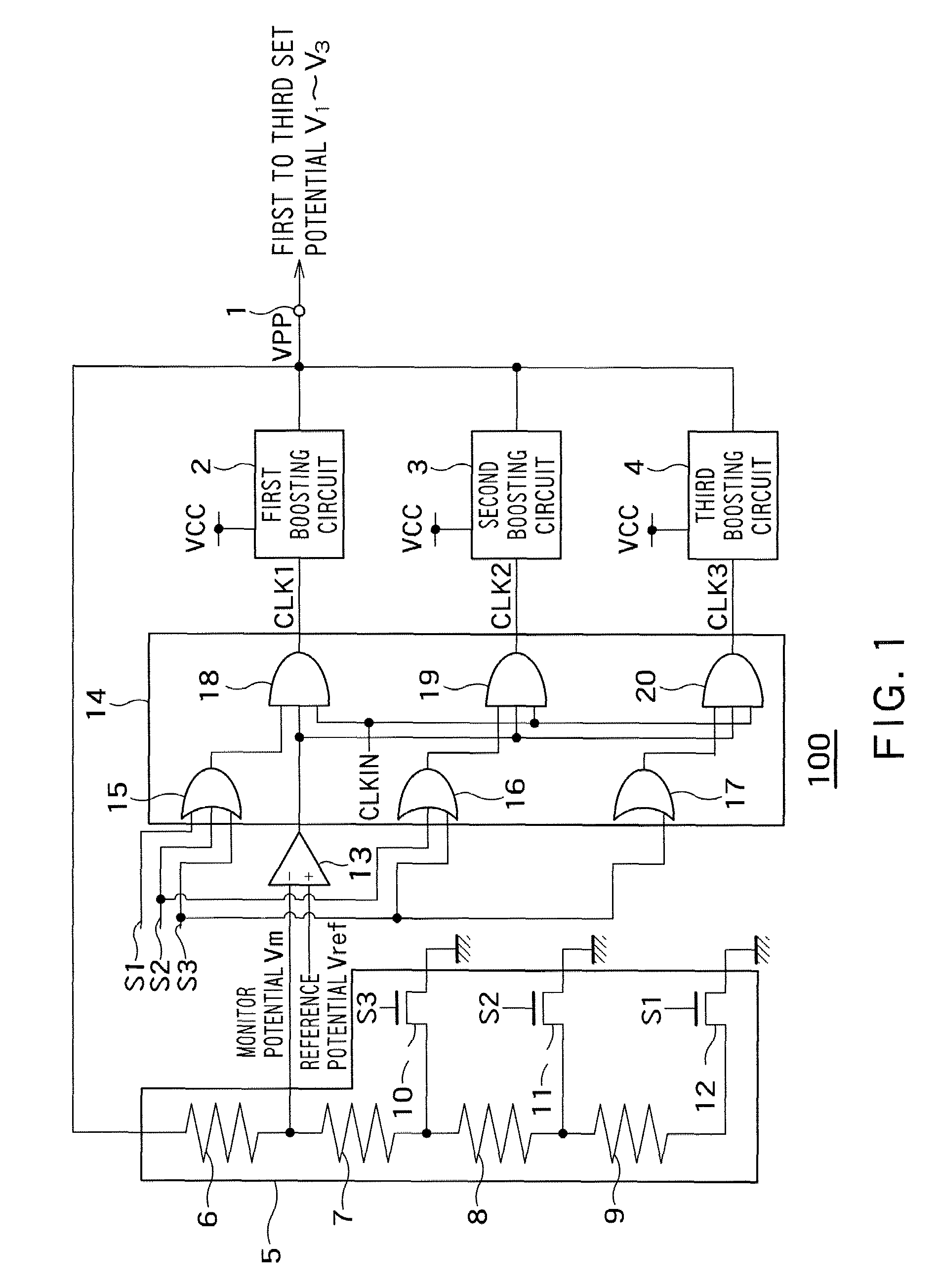
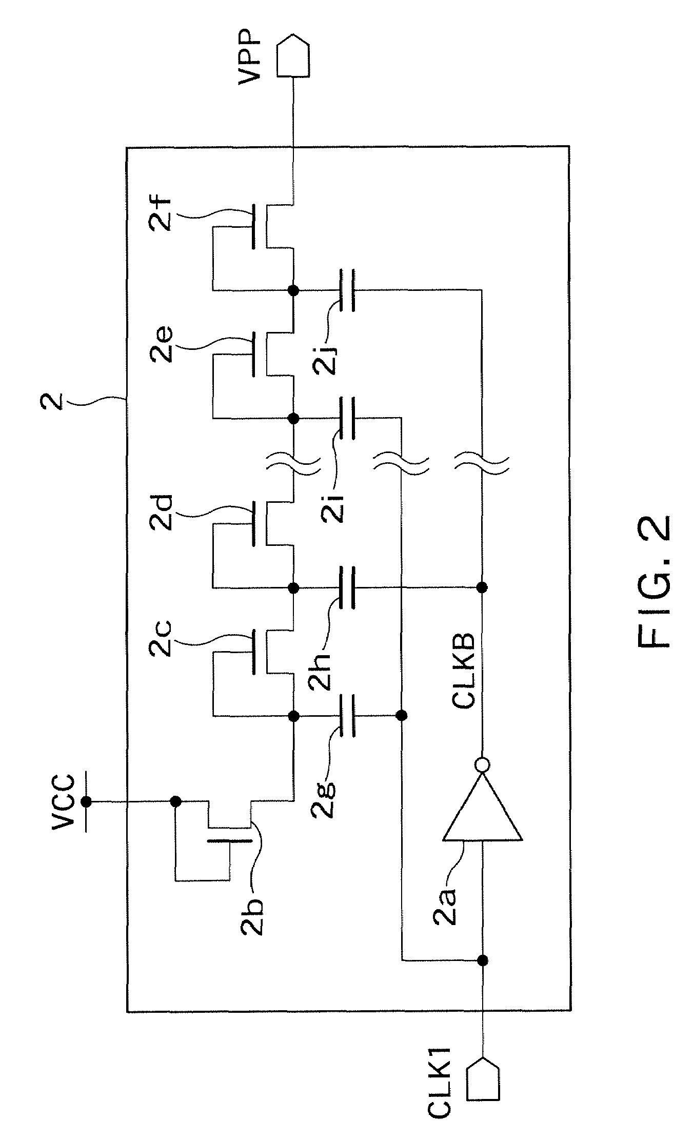
[0038]FIG. 1 is a figure showing an arrangement of a power source circuit 100 according to an embodiment as an aspect of the present invention. FIG. 2 is a figure showing an example of a boosting circuit applied to the power source circuit shown in FIG. 1.

[0039]As shown in FIG. 1, the power source circuit 100 outputs one of a first set potential V1, a second set potential V2, and a third set potential V3.

[0040]The first set potential V1 which is set according to a first selection signal S1. The second set potential V2 which is set according to a second selection signal S2 and is higher than the first set potential V1. The third set potential V3 which is set according to a third selection signal S3 and is higher than the second set potential V2.

[0041]As shown in FIG. 1, the power source circuit 100 includes an output terminal 1 which outputs one of the first set potential V1, the second set potential V2, and the third set potential V3, a first boosting circuit 2 which boosts a voltag...


PUM


Abstract

A power source circuit adapted to output a first set potential which is set according to a first selection signal, or a second set potential which is set according to a second selection signal and higher than the first set potential, has an output terminal adapted to output the first set potential or the second set potential; a first boosting circuit adapted to boost a voltage supplied from a power source and to output the boosted voltage to the output terminal; a second boosting circuit adapted to boost the voltage supplied from the power source and to output the boosted voltage to the output terminal; a voltage dividing circuit adapted to output a monitor potential by dividing the output potential outputted from the output terminal according to the first selection signal, or to output a monitor potential by dividing the output potential and reducing a voltage dividing ratio of the monitor potential with respect to the output potential according to the second selection signal; a comparison amplifier adapted to compare the monitor potential with a reference potential, and to output a flag signal for activating the boosting circuit when the monitor potential is lower than the reference potential; and a logic circuit adapted to receive the flag signal from the comparison amplifier, and when receiving the first selection signal, to output a first clock signal for making the first boosting circuit perform the boosting operation, and adapted to receive the flag signal from the comparison amplifier, and when receiving the second selection signal, to output a second clock signal for making the second boosting circuit perform the boosting operation, together with the first clock signal.

Description

CROSS-REFERENCE TO RELATED APPLICATION[0001]This application is based upon and claims the benefit of priority from the prior Japanese Patent Application No. 2006-138140, filed on May 17, 2006, the entire contents of which are incorporated herein by reference.BACKGROUND OF THE INVENTION[0002]1. Field of the Invention[0003]The present invention relates to a power source circuit provided with a boosting circuit for boosting power source voltage.[0004]2. Background Art[0005]Conventionally, a semiconductor storage device such as, for example, a NAND type flash memory is provided with a power source circuit which makes power source voltage boosted by a boosting circuit and supplied.[0006]For example, a semiconductor storage device, such as a NAND type flash memory, needs a potential higher than a power source voltage for data reading, writing and erasing operations. For this reason, such a semiconductor storage device is provided with a boosting circuit for boosting power source voltage a...

Claims


Application Information

Patent Timeline
Patent Type & Authority Patents(United States)
IPC IPC(8): G05F1/10
CPCH02M3/1584
Inventor TAKEYAMA, YOSHIKAZUSATO, JUMPEI
Owner KIOXIA CORP
Why Eureka
Try Eureka