Wiring board and method for producing the same
a technology of wired electrodes and wired components, which is applied in the manufacture of printed circuits, printed circuit aspects, solid-state devices, etc., can solve the problems of inability to meet the and the likelihood of failure in the connection between the electrode pad and the protruding electrode, so as to achieve the effect of suppressing the non-uniform height of protruding electrodes
- Summary
- Abstract
- Description
- Claims
- Application Information
AI Technical Summary
Benefits of technology
Problems solved by technology
Method used
Image

Examples
embodiment 1
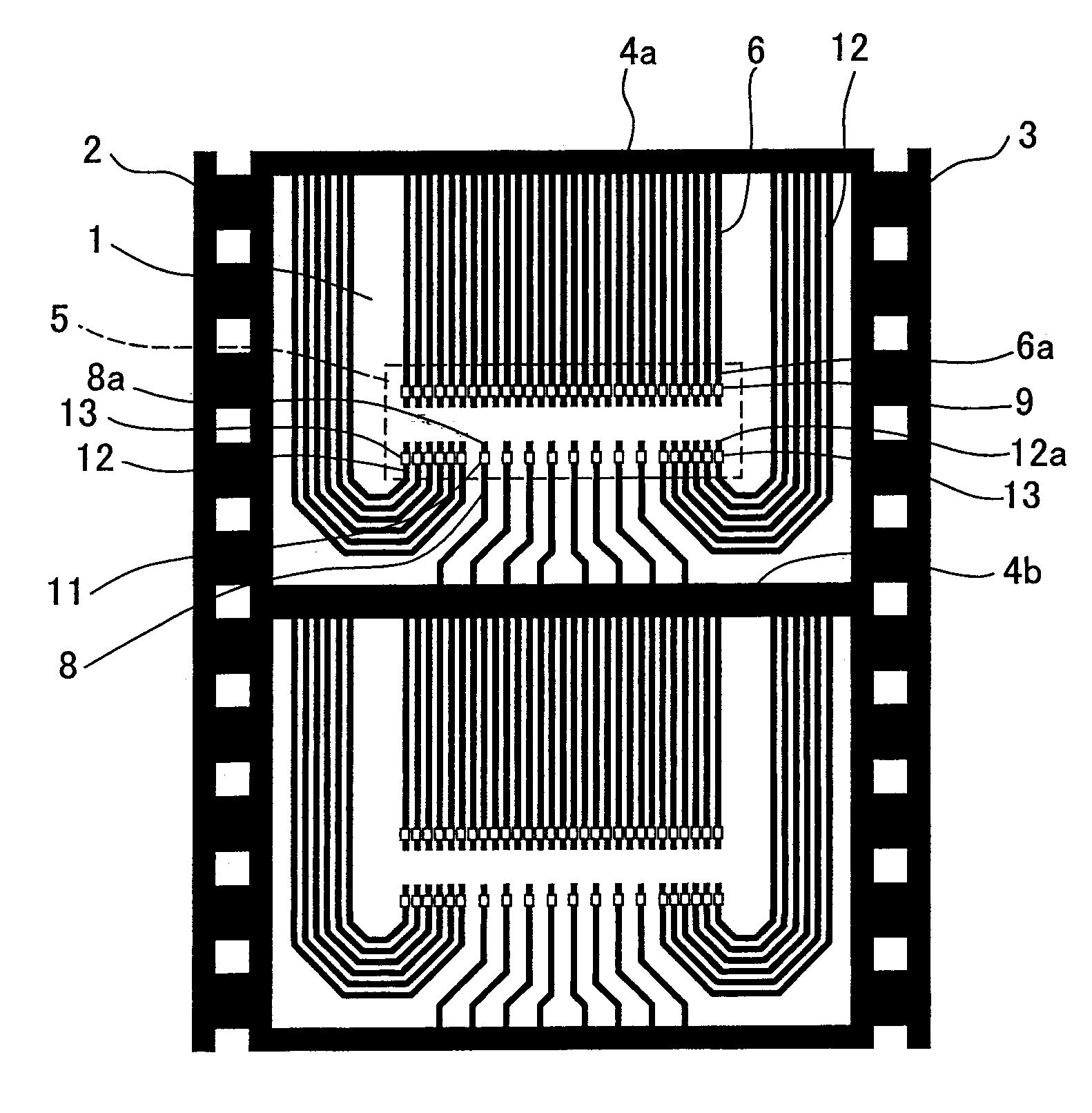
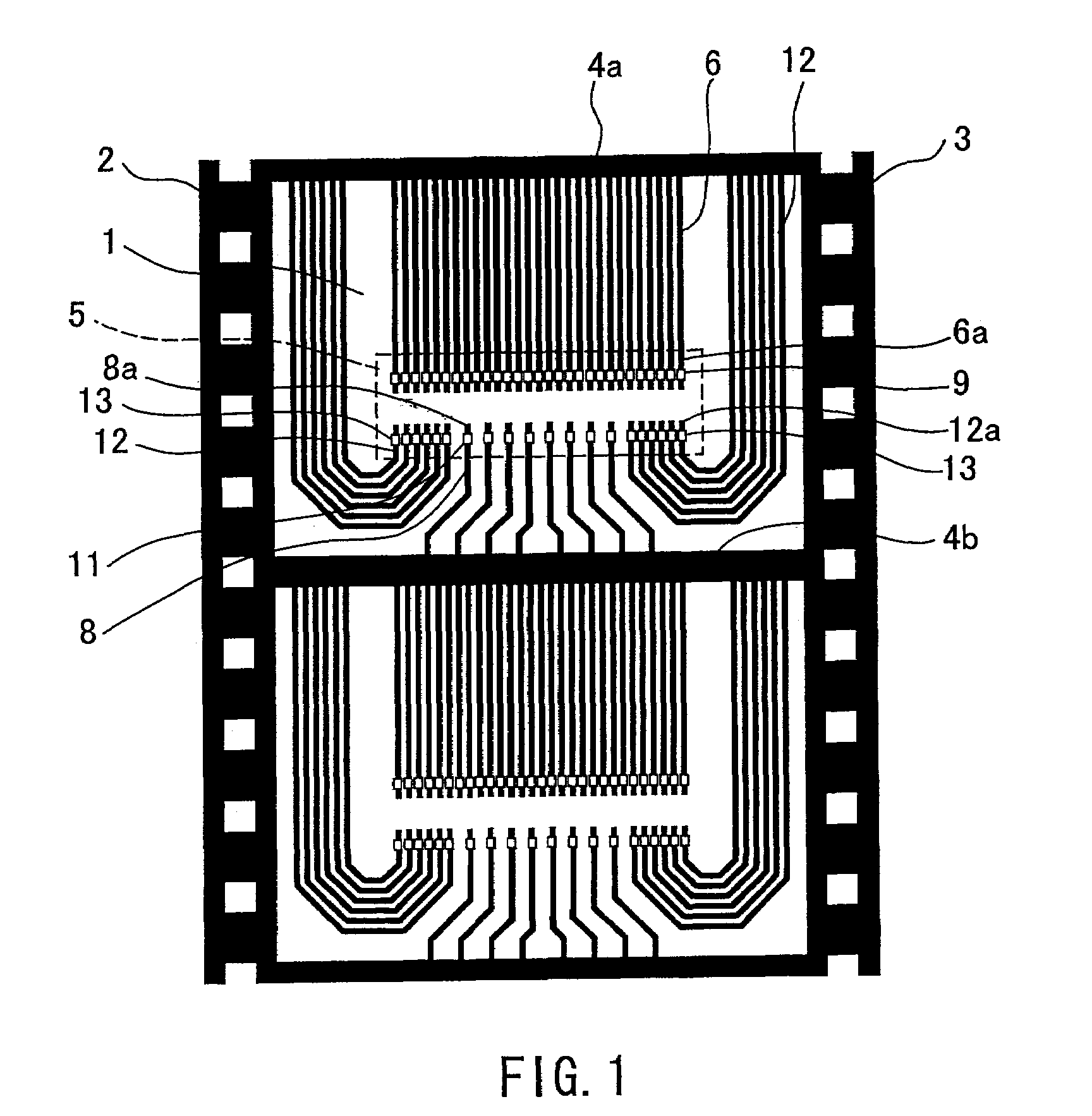
[0046]FIG. 1 is a plan view of a wiring board according to Embodiment 1. The basic structure of the wiring board of FIG. 1 is similar to the conventional example of FIG. 10. The same elements are indicated by the same reference numerals.
[0047]On a flexible and insulating substrate 1, first and second feeding electrodes 2 and 3 are formed, extending along both side edges in a longitudinal direction thereof. A plurality of feeding bus lines 4a, 4b are formed, extending in a traverse direction of the insulating substrate 1, and are connected to the first and second feeding electrodes 2 and 3. The feeding bus lines 4a, 4b section the insulating substrate 1 into a plurality of unit regions. A semiconductor chip mount portion 5 is provided in each unit region.
[0048]A plurality of conductor wirings 6, 8 and 12 are formed on the insulating substrate 1 for each unit region. Inner leads 6a, 8a and 12a formed by one-side end portions of the conductor wirings 6, 8 and 12 are arranged and aligne...
embodiment 2
[0083]FIG. 6 is a plan view of a wiring board according to Embodiment 2. The same parts as those of the wiring board of Embodiment 1 of FIG. 1 are indicated by the same reference numerals and the explanation thereof will not be repeated.
[0084]In this embodiment, there are two kinds of feeding bus lines, i.e., first feeding bus lines 14 and second feeding bus lines 15. The first feeding bus line 14 extends in a traverse direction of the insulating substrate 1, is connected to the first feeding electrode 2, but is not connected to the second feeding electrode 3. The second feeding bus line 15 extends in the traverse direction of the insulating substrate 1, is connected to the second feeding electrode 3, but is not connected to the first feeding electrode 2. The first and second feeding bus lines 14 and 15 section the insulating substrate 1 into unit regions.
[0085]The conductor wirings 6 and 12 forming the inner leads 6a of the first group and the inner leads 12a in the dense pitch reg...
embodiment 3
[0088]FIG. 8 is a plan view of a wiring board according to Embodiment 3. The same parts as those of the wiring board of Embodiment 2 of FIG. 4 are indicated by the same reference numerals and will not be described again.
[0089]In this embodiment, the first feeding bus line 14 has a width larger than that of the second feeding bus line 15, thereby making it possible readily to cause a power feeding current from the first feeding bus line 14 to be larger than a power feeding current from the second feeding bus line 15 when electrolytic plating is performed. Since the inner leads 6a and 12a having a dense wiring pitch are connected to the first feeding bus line 14 and the inner leads 8a having a sparse pitch are connected to the second feeding bus line 15, current density is caused to be uniform substantially in the entirety of a portion in which protruding electrodes are formed. Therefore, it is possible to suppress a difference in height between the protruding electrodes formed by ele...
PUM
 Abstract
Description
Claims
Application Information
 - R&D
- Intellectual Property
- Life Sciences
- Materials
- Tech Scout
- Unparalleled Data Quality
- Higher Quality Content
- 60% Fewer Hallucinations
Browse by: Latest US Patents, China's latest patents, Technical Efficacy Thesaurus, Application Domain, Technology Topic, Popular Technical Reports.
© 2025 PatSnap. All rights reserved.Legal|Privacy policy|Modern Slavery Act Transparency Statement|Sitemap|About US| Contact US: help@patsnap.com