Method of optimizing customizable filler cells in an integrated circuit physical design process

a technology of integrated circuits and filler cells, applied in computer aided design, program control, instruments, etc., can solve the problems of inability to control the location of potential customizable filler cells, inability to incorporate customizable filler cells within the overall circuit design, and gaps or empty spaces between certain adjacent logic cells, so as to reduce the traceability of electronic messages

Active Publication Date: 2008-10-28
GLOBALFOUNDRIES U S INC
View PDF10 Cites 205 Cited by
  • Summary
  • Abstract
  • Description
  • Claims
  • Application Information

AI Technical Summary

Problems solved by technology

Additionally, there may exist gaps or empty spaces between certain adjacent logic cells.
Because the locations, sizes, and number of the empty spaces within a circuit design layout, which is the result of the placement algorithms in the logic synthesis operation, is random, the ability to incorporate customizable filler cells within the overall circuit design is not controlled.
In particular, the locations of potential customizable filler cells are not controlled, in that, they may be clustered in one area only of the overall circuit layout or be distributed poorly (e.g., located at the perimeter only of the overall circuit layout).
Consequently, the usefulness of the resulting customizable filler cells that exist in random locations, numbers, and distribution within the circuit design, for implementing circuit modifications, is limited.

Method used


Image

  • Method of optimizing customizable filler cells in an integrated circuit physical design process
  • Method of optimizing customizable filler cells in an integrated circuit physical design process
  • Method of optimizing customizable filler cells in an integrated circuit physical design process

Examples


Embodiment Construction

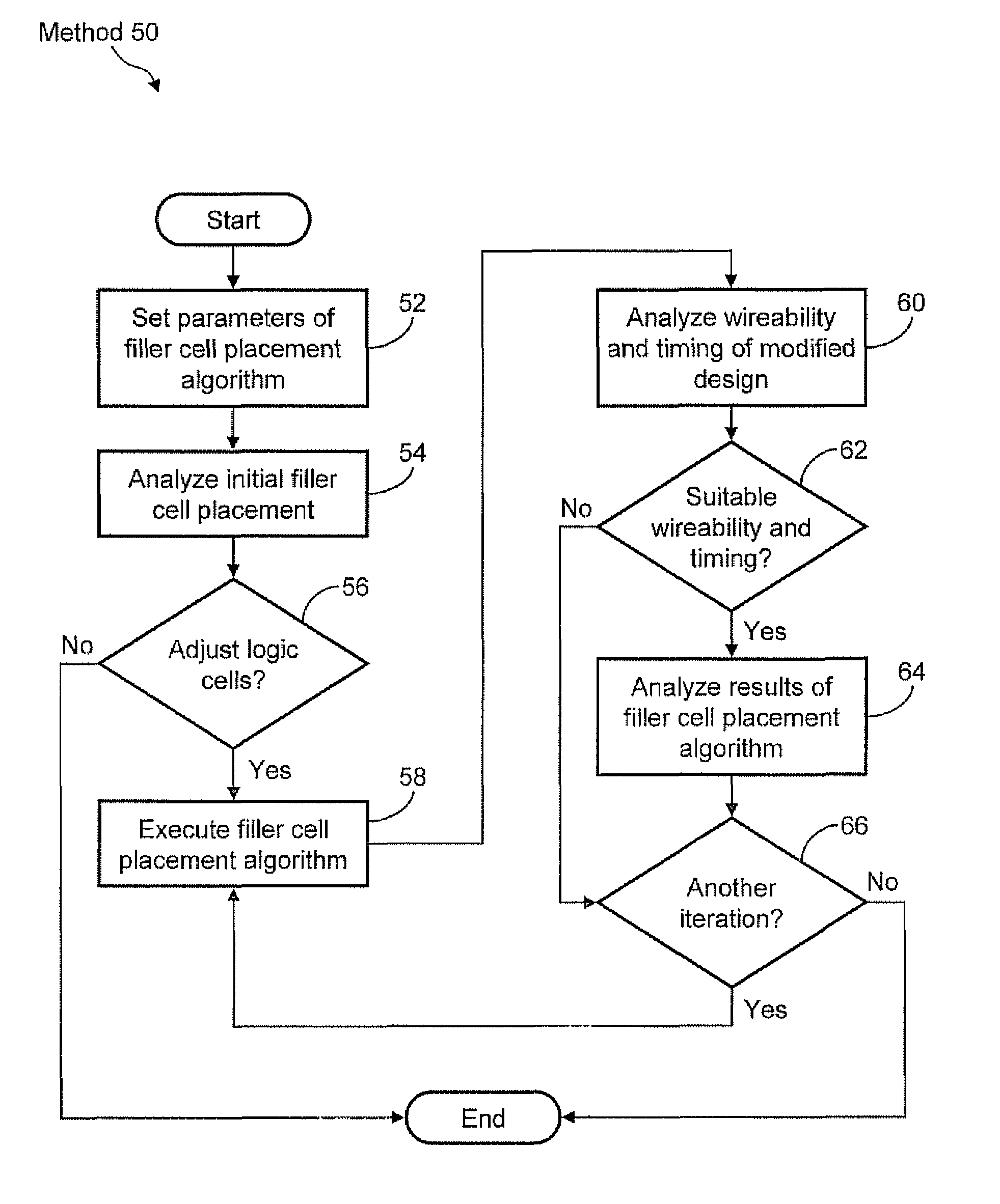
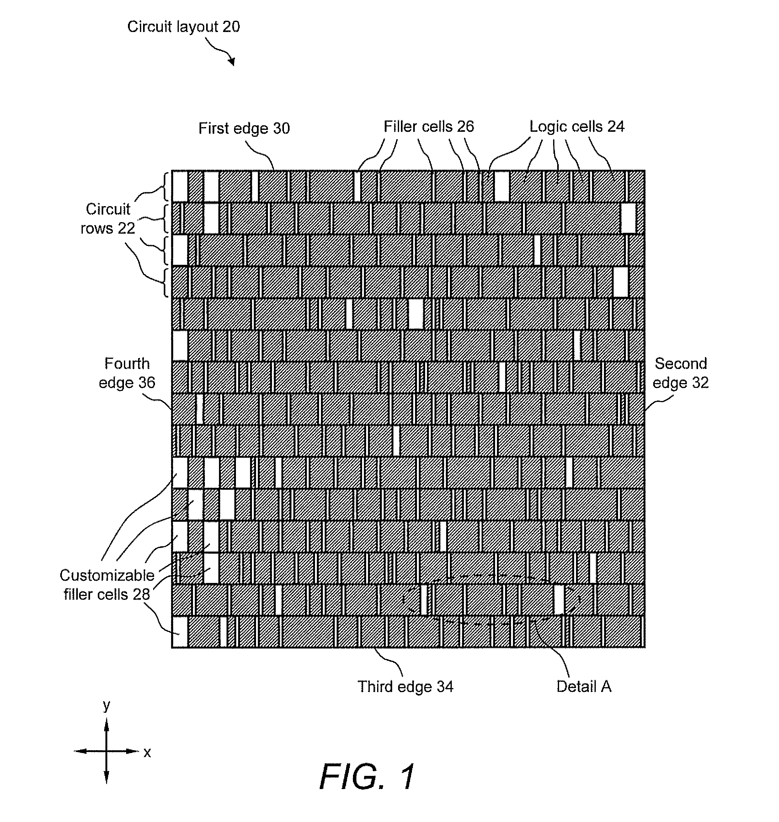
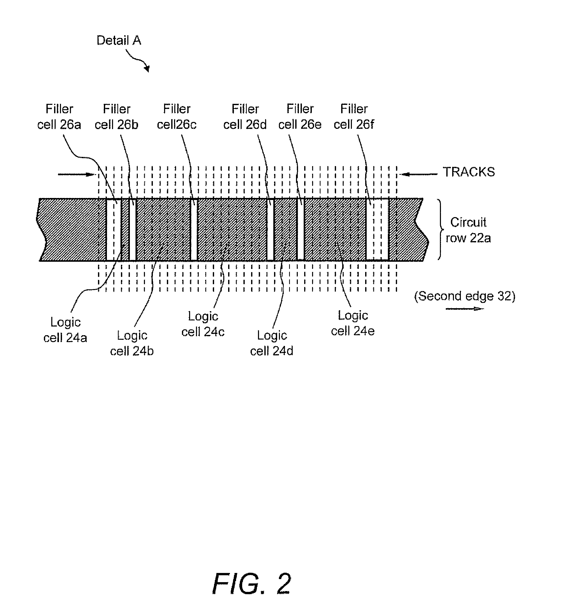
[0017]FIG. 1 illustrates a circuit layout 20, which is a representative of arbitrary circuit layouts that result from a standard logic synthesis operation. Circuit layout 20 includes a plurality of circuit rows 22 that each further includes a plurality of logic cells 24 that have a plurality of filler cells 26 and / or customizable filler cells 28 distributed randomly therein. The collective arrangement of circuit rows 22 forms the overall physical design of circuit layout 20, as shown in FIG. 1. As a result, circuit layout 20 has a first edge 30, a second edge 32, a third edge 34, and a fourth edge 36. Those skilled in the art will recognize that circuit layout 20 may be formed, alternatively, of circuit columns or other regions. The formation of circuit layout 20 by use of circuit rows 22 is exemplary only, and the method may be implemented with respect to regions in the circuit layout other than circuit rows.

[0018]Logic cells 24 represent a collection of specific logic functions, a...


PUM


Abstract

A system and method for optimizing customizable filler cells in an integrated circuit physical design process. In particular, a filler cell placement algorithm of the present disclosure is utilized in the method to optimize the customizable filler cells in a circuit layout. The filler cell placement algorithm performs the operation of selecting a starting point within a given circuit layout, selecting a direction in which the position of logic cells is adjusted, adjusting the position of logic cells and, thereby, combining filler cells in order to increase the accumulated area thereof; suspending the adjustment operation when a customizable filler cell is formed; and resuming the adjustment operation from the point of the newly formed customizable filler cell. Additionally, a method of optimizing the locations, number, and distribution of the customizable filler cells in an integrated circuit design by use of the filler cell placement algorithm is provided.

Description

FIELD OF THE INVENTION[0001]The present invention generally relates to the field of integrated circuit physical design. In particular, the present invention is directed to a system for and method of optimizing customizable filler cells in an integrated circuit physical design process.BACKGROUND[0002]Logic synthesis is a computer process that transforms a circuit description from one level of abstraction to a lower level, usually towards the physical implementation of an integrated circuit. As a result of the logic synthesis process, logic cells or logic functions are arranged physically in multiple circuit rows and / or circuit columns in order to form the completed design. Furthermore, each circuit row and / or circuit column contains multiple logic cells that are arranged adjacent one to another.[0003]Additionally, there may exist gaps or empty spaces between certain adjacent logic cells. These empty spaces, sometimes referred to as “white spaces,” exist in random locations and are of...

Claims


Application Information

Patent Timeline
Patent Type & Authority Patents(United States)
IPC IPC(8): G06F17/50
CPCG06F17/5072G06F30/392
Inventor CHARLEBOIS, STEVEN E.DUNN, PAUL E.ROHRBAUGH, III, GEORGE W.
Owner GLOBALFOUNDRIES U S INC
Why Eureka
Try Eureka