Design stage mitigation of interconnect variability

a technology of interconnect variability and design stage, applied in the direction of program control, total factory control, instruments, etc., can solve the problems of affecting interconnect signal delay and crosstalk, affecting the design range of wire thickness of these nets, and regions in layout cannot reach the required metal density, so as to mitigate the effects of interconnect variability and mitigate the effect of interconnect variability

Active Publication Date: 2008-11-04
GLOBALFOUNDRIES U S INC
View PDF10 Cites 20 Cited by
  • Summary
  • Abstract
  • Description
  • Claims
  • Application Information

AI Technical Summary

Benefits of technology

[0008]A first aspect of the present invention provides a method for mitigating effects of interconnect variability of a chip, comprising: performing global and detailed routing of interconnects of the chip; and during a design stage of the chip: performing dummy fill estimation based on the global and detailed routing of the interconnects; performing grid based metal density estimation; and obtaining a variable map of metal thicknesses.
[0009]A second aspect of the present invention provides a computer-implemented method for mitigating effects of interconnect variability during a design stage of a chip, comprising: performing global and detailed routing of interconnects of the chip; performing dummy fill estimation based on the global and detailed routing of the interconnects; performing grid based metal density estimation; obtaining a variable map of metal thicknesses; identifying wiring nets of the chip that are sensitive to metal variability based on the variable map of metal thicknesses; and re-routing the wiring nets during the design stage for optimization of the chip.
[0010]A third aspect of the present invention provides a system for mitigating effects of interconnect variability during a design stage of a chip, comprising: a routing system for performing global and detailed routing of interconnects of the chip; a dummy fill estimation system for performing dummy fill estimation based on the global and detailed routing of the interconnects; a density estimation system for performing grid based metal density estimation; a variable mapping system for obtaining a variable map of metal thicknesses; a net identification system for identifying wiring nets of the chip that are sensitive to metal variability based on the variable map of metal thicknesses; and an optimization system for re-routing the wiring nets during the design stage for optimization of the chip.
[0011]A fourth aspect of the present invention provides a program product stored on a computer readable medium for mitigating effects of interconnect variability during a design stage of a chip, the computer readable medium comprising program code for causing a computer system to perform the following steps: performing global and detailed routing of interconnects of the chip; performing dummy fill estimation based on the global and detailed routing of the interconnects; performing grid based metal density estimation; obtaining a variable map of metal thicknesses; identifying wiring nets of the chip that are sensitive to metal variability based on the variable map of metal thicknesses; and re-routing the wiring nets during the design stage for optimization of the chip.
[0014]Therefore, the present invention provides a technique for mitigating effects of interconnect variability during a design stage of a chip.

Problems solved by technology

Although these techniques can improve the layout density evenness, the introduction of millions of dummy fills and cheese holes may affect interconnect signal delay and crosstalk due to the resistance and the coupling capacitance changes.
Moreover, it is highly likely that some regions in the layout cannot reach the required metal density even with dummy fills or cheesing holes.
Still yet, if there are critical nets that traverse these regions, the wire thickness of these nets may be out of the design range due to the thickness loss / gain caused by the CMP process.
As such, these nets may fail to meet the timing closure.

Method used


Image

  • Design stage mitigation of interconnect variability
  • Design stage mitigation of interconnect variability
  • Design stage mitigation of interconnect variability

Examples


Embodiment Construction

[0028]For convenience purposes, the Detailed Description of the Invention will have the following sections:

[0029]I. General Description

[0030]II. Illustrative Embodiment

[0031]III. Computerized Implementation

I. General Description

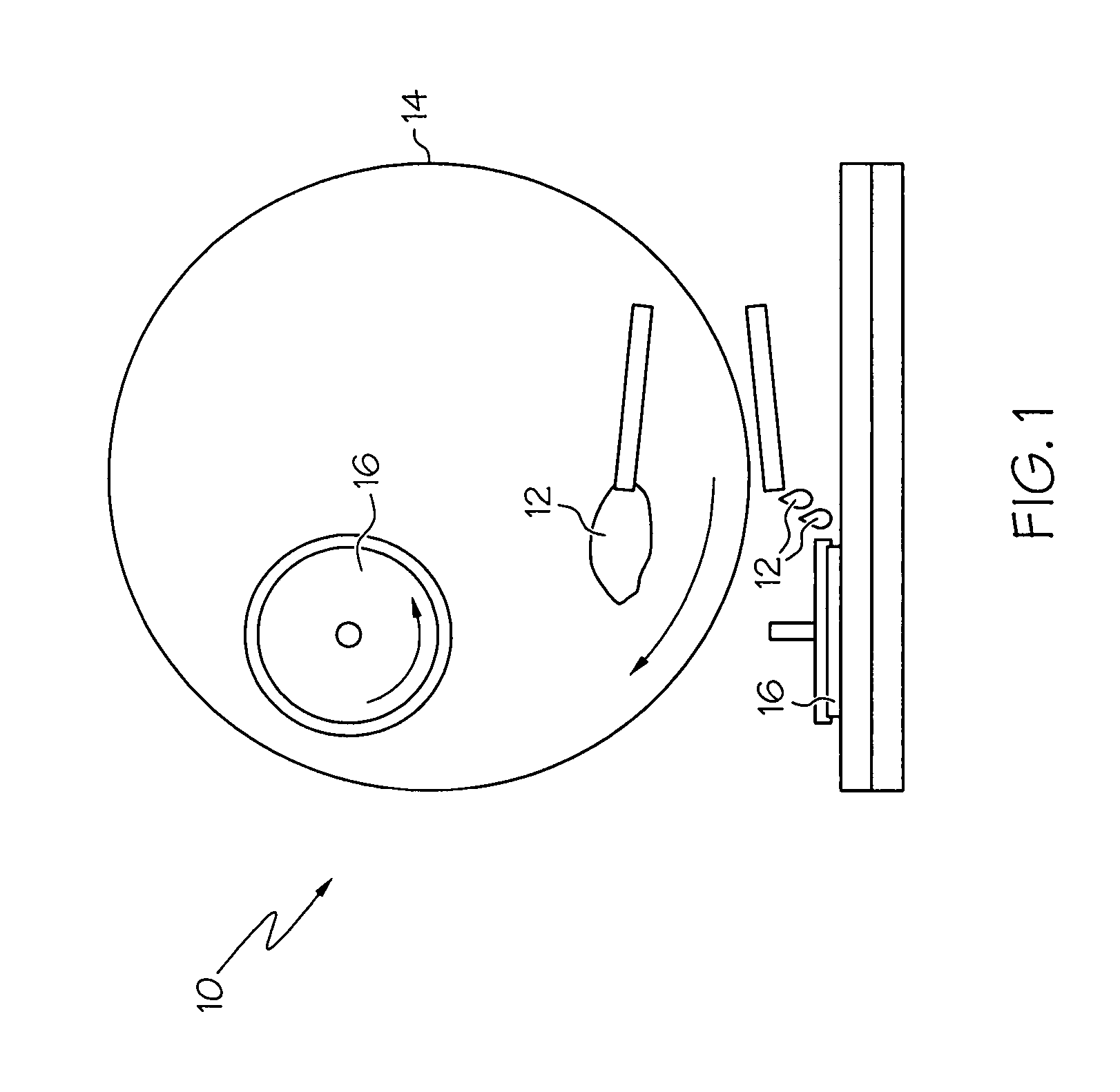
[0032]As indicated above, the design of chips is often adversely affected by variability in the back end of the line (BEOL). That is, mismatching commonly occurs between the design and manufacturing stages of the chip. One manufacturing stage technique where such variability is typically caused is Chemical-Mechanical Polishing (CMP). Referring to FIG. 1, a diagram 10 of a known CMP process is shown. As depicted, a slurry 12 is distributed at various positions along a polishing pad 14. As force is applied against a chip or wafer 16, the rotational motion of polishing pad 14 causes chip 16 to be polished or planarized. While CMP can be necessary to establish reliable multilevel interconnects, CMP needs to be closely controlled to avoid the aforementioned advers...


PUM


Abstract

The present invention provides a method, system and program product for mitigating effects of interconnect variability during a design stage of a chip. Under the technique of the present invention, a global and detailed routing of interconnects of the chip are determined. Thereafter, a dummy fill estimation and a grid based metal density estimation are performed. Then, based on a CMP model, a variable map of metal thicknesses is obtained. Based on the variable map, wiring nets of the chip that are sensitive to metal variability (e.g., that fail to meet timing closure due to metal thickness loss / gain in the CMP process) are identified. These wiring nets are then re-routed for optimization of the chip.

Description

BACKGROUND OF THE INVENTION[0001]1. Field of the Invention[0002]The present invention generally relates to mitigation of interconnect variability of an integrated circuit (“chip”). Specifically, the present invention provides a way to mitigate interconnect variability of a chip during its design stage.[0003]2. Related Art[0004]In nanometer-scale Very Large-Scale Integration (VLSI), the design of a chip is increasingly affected by the variability in the back end of the line (BEOL), or interconnect resistance and capacitance. The mismatch between design and manufacturing has to be well controlled in order to guarantee performance and manufacturability. Chemical-Mechanical Polishing (CMP) is widely used as a primary technique in modern integrated circuit fabrication. In this process, after depositing one layer of material on previous layers of material along with an insulating dielectric, CMP is used to planarize the surface layer. Global planarization is typically necessary for establ...

Claims


Application Information

Patent Timeline
Patent Type & Authority Patents(United States)
IPC IPC(8): G06F17/50
CPCG06F17/5068G06F2217/12G06F30/39G06F2119/18Y02P90/02
Inventor LAVIN, MARK A.PURI, RUCHIRTREVILLYAN, LOUISE H.XIANG, HUA
Owner GLOBALFOUNDRIES U S INC
Why Eureka
Try Eureka