Method for dividing substrate

a substrate and dividing technology, applied in the direction of lasers, semiconductor laser structural details, semiconductor lasers, etc., can solve the problems of increasing the cost of chips, reducing the total number of chips obtained from one substrate, and frequent occurrence of chip breaking, so as to achieve low cost and high yield. , the effect of low cos

Inactive Publication Date: 2008-12-02
PANASONIC CORP
View PDF22 Cites 122 Cited by
  • Summary
  • Abstract
  • Description
  • Claims
  • Application Information

AI Technical Summary

Benefits of technology

[0015]In view of the above technical problems, it is an object of the present invention to provide a method for dividing a substrate that is (i) applicable to a cleavage method and a chip separation method for a semiconductor substrate, (ii) capable of dividing each substrate into chips in the same square-like form without causing chip breaking, and (iii) capable of forming all cleaved facets flat.
[0053]As described above, it is possible for the present invention to provide a method for dividing a substrate that is capable of dividing each substrate into chips in the same square-like form without causing chip breaking as well as capable forming all cleaved facets flat. The present invention particularly makes it possible to divide each substrate into chips in the same square-like form without causing chip breaking and to form all cleaved facets flat in dividing a substrate that includes a rigid substrate, such as a sapphire substrate and a SiC substrate, and a nitride semiconductor device formed on such rigid substrate. What is more, since there hardly ever occurs breaking in a scribed line part on the substrate, it becomes possible to increase a total number of chips manufactured from one substrate and therefore to perform a manufacture process at low cost. Furthermore, it becomes also possible to easily divide a substrate including a highly rigid low dielectric film that is beginning to be used as a substrate for the state-of-the-art Si-LSI, by cleaving the Si substrate after causing cleavage inside the low dielectric film.

Problems solved by technology

However, the conventional method for dividing a semiconductor substrate has problems such as that there is a frequent occurrence of chip breaking and chips cannot be cut in the same square-like form since such conventional method, in any cases shown in FIG. 1A, FIG. 1B, and FIG. 2, requires the formation of ditches on the semiconductor substrate using a diamond scriber or the like, or requires the cutting of the semiconductor substrate.
Furthermore, since chip separation by means of cutting with a diamond blade requires a room for a chip width to be cut by the diamond blade, there is also a problem that a total number of chips obtained from one substrate is decreased and the cost of chips is increased.
Furthermore, since it is difficult to obtain a flat cleaved facet when performing cleavage to form a resonator of a semiconductor laser element, there is a problem that the threshold current of the semiconductor laser element becomes higher and the process yield becomes worse.

Method used


Image

  • Method for dividing substrate
  • Method for dividing substrate
  • Method for dividing substrate

Examples


first embodiment

[0071]FIG. 3 is a cross-sectional view showing a method for cleaving a nitride semiconductor substrate according to the first embodiment of the present invention. Referring to FIG. 3 to FIG. 9, a description is given below of a condition for electron beam irradiation that allows all cleaved facets to be formed flat.

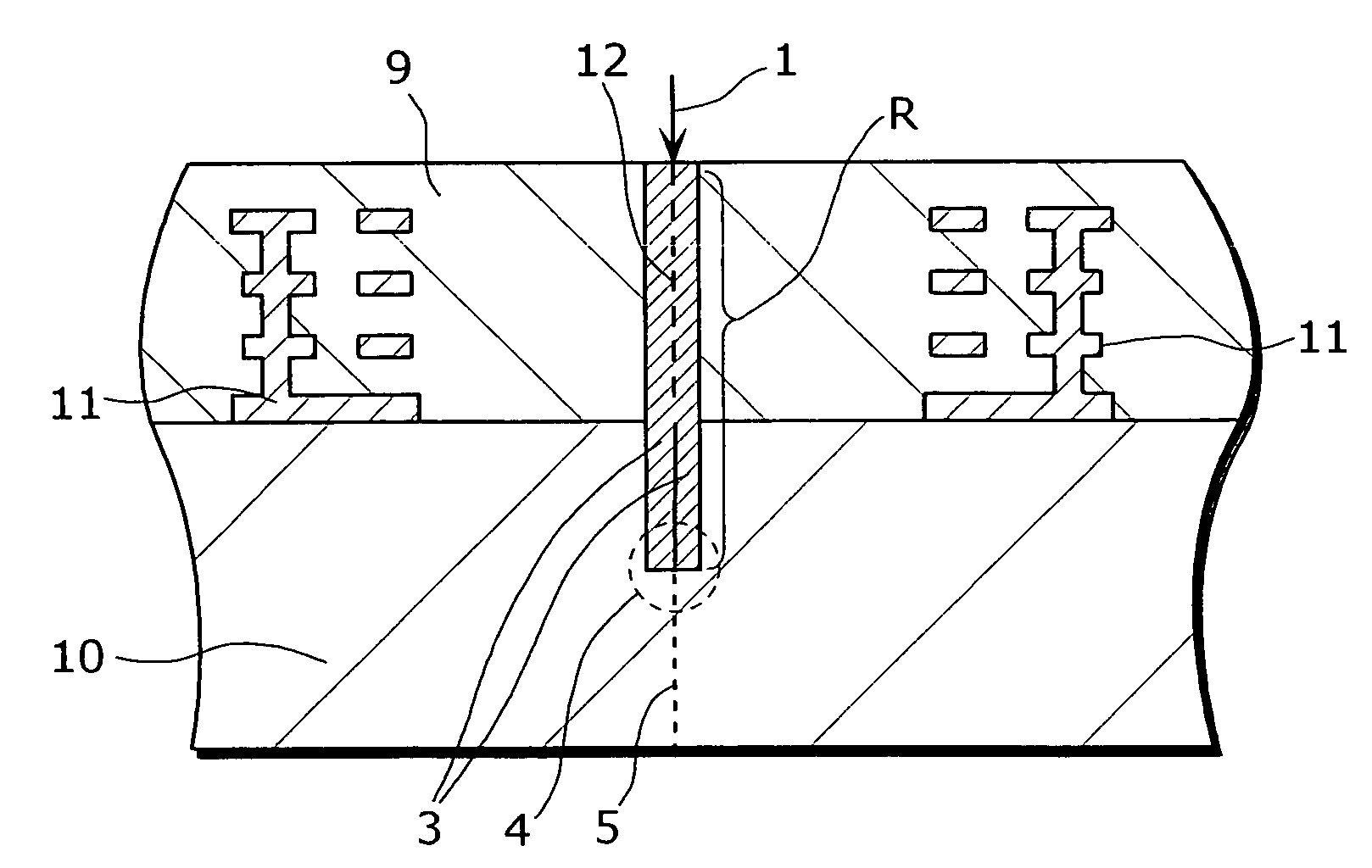
[0072]As shown in FIG. 3, an electron beam 1 is irradiated to a substrate surface 2 of a nitride semiconductor substrate under an irradiation condition made up of an acceleration voltage Vb, a beam current Ib, and an electron beam energy Eb. In this case, a beam radius that depends on the above irradiation condition is db. The electron beam 1 reaches the full depth of a projected range R from the substrate surface 2. This projected range R is defined by the depth from the substrate surface 2 to the position at which the electron strength becomes 0. In this case, since the acceleration voltage of the electron beam 1 to be irradiated is a relatively low acceleration voltage...

second embodiment

[0084]FIG. 10 is a cross-sectional view showing a method for cleaving a nitride semiconductor substrate according to the second embodiment of the present invention.

[0085]As shown in FIG. 10, an electron beam 1 is irradiated to the front surface of a nitride semiconductor substrate made up of a sapphire substrate 7 and a GaN-based semiconductor thin film 6 formed on such sapphire substrate 7. The GaN-based semiconductor thin film 6 forms, for example, a semiconductor laser element or a light-emitting diode. Note that an electrode or the like may be previously formed on the GaN-based semiconductor thin film 6. The present embodiment has a structure in which the projected range R of the electron beam 1 reaches inside the sapphire substrate 7 located under the GaN-based semiconductor thin film 6 and cleavage as described in the first embodiment starts from the sapphire substrate 7. Although there occurs a crack in the GaN-based semiconductor thin film 6 even in the case where the electr...

third embodiment

[0086]FIG. 11 is a cross-sectional view showing a method for cleaving a nitride semiconductor substrate according to the third embodiment of the present invention.

[0087]As shown in FIG. 11, an electron beam 1 is irradiated to the front surface of a nitride semiconductor substrate made up of a sapphire substrate 7 and a GaN-based semiconductor thin film 6 formed on such sapphire substrate 7. The GaN-based semiconductor thin film 6 forms, for example, a semiconductor laser element or a light-emitting diode. Note that an electrode or the like may be previously formed on the GaN-based semiconductor thin film 6. The electron beam 1 is irradiated from the front surface of the GaN-based semiconductor thin film 6 in the second embodiment, but the present embodiment has a structure in which the nitride semiconductor substrate is cleaved by irradiating the electron beam 1 from the side of the sapphire substrate 7. Since the electron beam 1 is not irradiated from the side of the GaN-based semi...


PUM


Abstract

The present invention aims at providing a method for dividing a substrate that is capable of dividing each substrate into chips in the same square-like form without causing chip breaking and capable of forming all cleaved facets flat. In the method for dividing a substrate of the present invention, an electron beam 1 with the intensity that causes a dislocation inside the substrate is irradiated to a substrate surface 2 to generate a crack starting from such dislocation, and a cleaved facet 5 is formed to divide the substrate.

Description

BACKGROUND OF THE INVENTION[0001](1). Field of the Invention[0002]The present invention relates to a method for dividing a substrate that is applicable to a method for manufacturing, for example, a semiconductor laser element, a light-emitting diode, and a field-effect transistor integrated circuit that are made up of nitride semiconductors.[0003](2). Description of the Related Art[0004]A GaN-based nitride semiconductor (InGaAIN), which is represented by the composition formula AlxGa1-x-yInyN (0≦x≦1, 0≦y≦1, 0≦z≦1, 0≦x+y+z≦1) and has a wide band gap (the band gap width of GaN at room temperature is 3.4 eV), is a material that can realize a high-power light-emitting diode in a wavelength range such as the green / blue visible range and the ultraviolet region. A widely used light-emitting diode realized by InGaAIN is a white light-emitting diode that obtains white light by exciting a fluorescent substance by a blue light-emitting diode. Furthermore, a violet semiconductor laser element u...

Claims


Application Information

Patent Timeline
Patent Type & Authority Patents(United States)
IPC IPC(8): H01L21/44H01L21/301H01L21/304H01L21/78H01L33/00H01S5/02H01S5/343
CPCB82Y20/00H01L21/3043H01S5/0201H01S5/34333H01L21/78H01L33/0095H01S5/0213
Inventor UEDA, TETSUZOUEDA, DAISUKE
Owner PANASONIC CORP
Why Eureka
Try Eureka