Semiconductor memory device
a memory device and semiconductor technology, applied in the field of semiconductor memory devices, can solve the problems of data not being held within the refresh test time, memory cells becoming defective, and disturb refresh test time occupying a large proportion of memory test time, so as to reduce the disturb refresh test time
- Summary
- Abstract
- Description
- Claims
- Application Information
AI Technical Summary
Benefits of technology
Problems solved by technology
Method used
Image
Examples
first embodiment
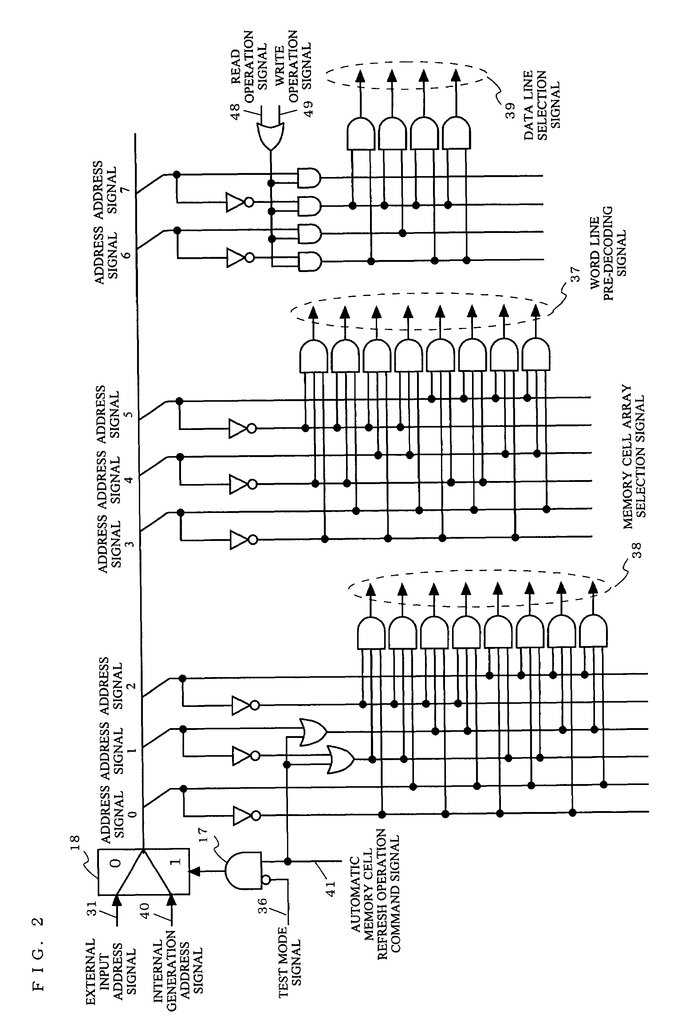
[0026]FIG. 2 is a diagram illustrating an exemplary configuration of a row pre-decoding circuit 16 according to a first embodiment of the present invention. The row pre-decoding circuit 16 according to the first embodiment is different from the conventional row pre-decoding circuit 56 in that the row pre-decoding circuit 16 includes a logic element 17 in which a test mode signal 36 is inputted and a logical product of an inversion signal of the test mode signal 36 and the automatic memory cell refresh operation command signal 41 is found.
[0027]When the row pre-decoding circuit 16 according to the first embodiment operates in a normal mode, the test mode signal 36 is set at a low level. In the state of this normal mode, when the automatic memory cell refresh operation command signal 41 reaches a high level, the internally generated address signal 40 is selected in a selector 18. And when the automatic memory cell refresh operation command signal 41 reaches a high level, an address si...
second embodiment
[0037]FIG. 3 is a diagram illustrating an exemplary configuration of a row pre-decoding circuit 16 according to a second embodiment of the present invention. The row pre-decoding circuit 16 according to the second embodiment is different from the conventional row pre-decoding circuit 56 in that the row pre-decoding circuit 16 includes: a logic element 19 in which a test mode signal 36 is inputted and a logical product of a test mode signal 36 and a read operation signal 48 is found; and a logic element 20 in which a logical sum of an output of the logic element 19 and an automatic memory cell refresh operation command signal 41 is found.
[0038]When the row pre-decoding circuit 16 according to the second embodiment operates in a normal mode, the test mode signal 36 is set at a low level. In a state of this normal mode, a read operation, a write operation, and an automatic memory cell refresh operation are same as those in the above-described first embodiment.
[0039]Next, a case of a te...
third embodiment
[0049]FIG. 4 is a diagram illustrating an exemplary configuration of a row pre-decoding circuit 16 according to a third embodiment according to the present invention. The row pre-decoding circuit 16 according to the third embodiment is different from the conventional row pre-decoding circuit 56 in that the row pre-decoding circuit 16 includes a logic element 21 in which a test mode signal 36 is inputted and a logical sum of the test mode signal 36 and an automatic memory cell refresh operation command signal 41 is found.
[0050]The row pre-decoding circuit 16 in the third embodiment supports an RAS refresh operation for any memory cells by using an externally inputted address signal 31 as an externally inputted command. When the row pre-decoding circuit 16 in the third embodiment is set to be in a test mode state, the row pre-decoding circuit 16 is characterized in that memory cell arrays, the number of which is equal to that of the memory cell arrays which are activated in an automat...
PUM
 Abstract
Description
Claims
Application Information


