Bipolar transistor formed using selective and non-selective epitaxy for base integration in a BiCMOS process

a bicmos and base integration technology, applied in the field of bicmos and cmos device fabrication, can solve the problems of limited active area scaling in the conventional bicmos integration process, surface exposed, recesses of isolation regions, etc., and achieve the effect of reducing base-collector capacitance and base resistance, and increasing active area scalability

Active Publication Date: 2008-12-09
NEWPORT FAB +1
View PDF4 Cites 9 Cited by
  • Summary
  • Abstract
  • Description
  • Claims
  • Application Information

AI Technical Summary

Benefits of technology

[0009]The present invention is directed to selective and non-selective epitaxy for base integration in a BiCMOS process and related structure. The present invention overcomes the need in the art for a bipolar transistor in a BiCMOS process that provides increased active area scalability and reduced base-collector capacitance and base resistance.

Problems solved by technology

However, active area scaling is limited in a conventional BiCMOS integration process as a result of facet formation that occurs during a non-selective epitaxial process that is used for base layer formation.
However, the wet etch results in a recess of the isolation region such that a silicon surface is exposed.
As a result, during the subsequent base layer formation, typically involving a non-selective epitaxial deposition, the exposed silicon surface can cause uncontrolled facet formation, which causes an undesirable reduction in the usable area that is available for emitter formation.
Thus, in the conventional BiCMOS integration process, the performance route is well known, namely active scaling, but there exists a physical limitation in the implementation of active scaling due to facet formation at the isolation periphery.
Consequently, this route to reaching greater performance of power gain is limited by such an obstacle.
Moreover, the thin extrinsic base regions in the conventional bipolar transistor further contribute to the undesirable decrease in power gain in that the thin extrinsic base regions result in a higher base resistance.

Method used


Image

  • Bipolar transistor formed using selective and non-selective epitaxy for base integration in a BiCMOS process
  • Bipolar transistor formed using selective and non-selective epitaxy for base integration in a BiCMOS process
  • Bipolar transistor formed using selective and non-selective epitaxy for base integration in a BiCMOS process

Examples


Embodiment Construction

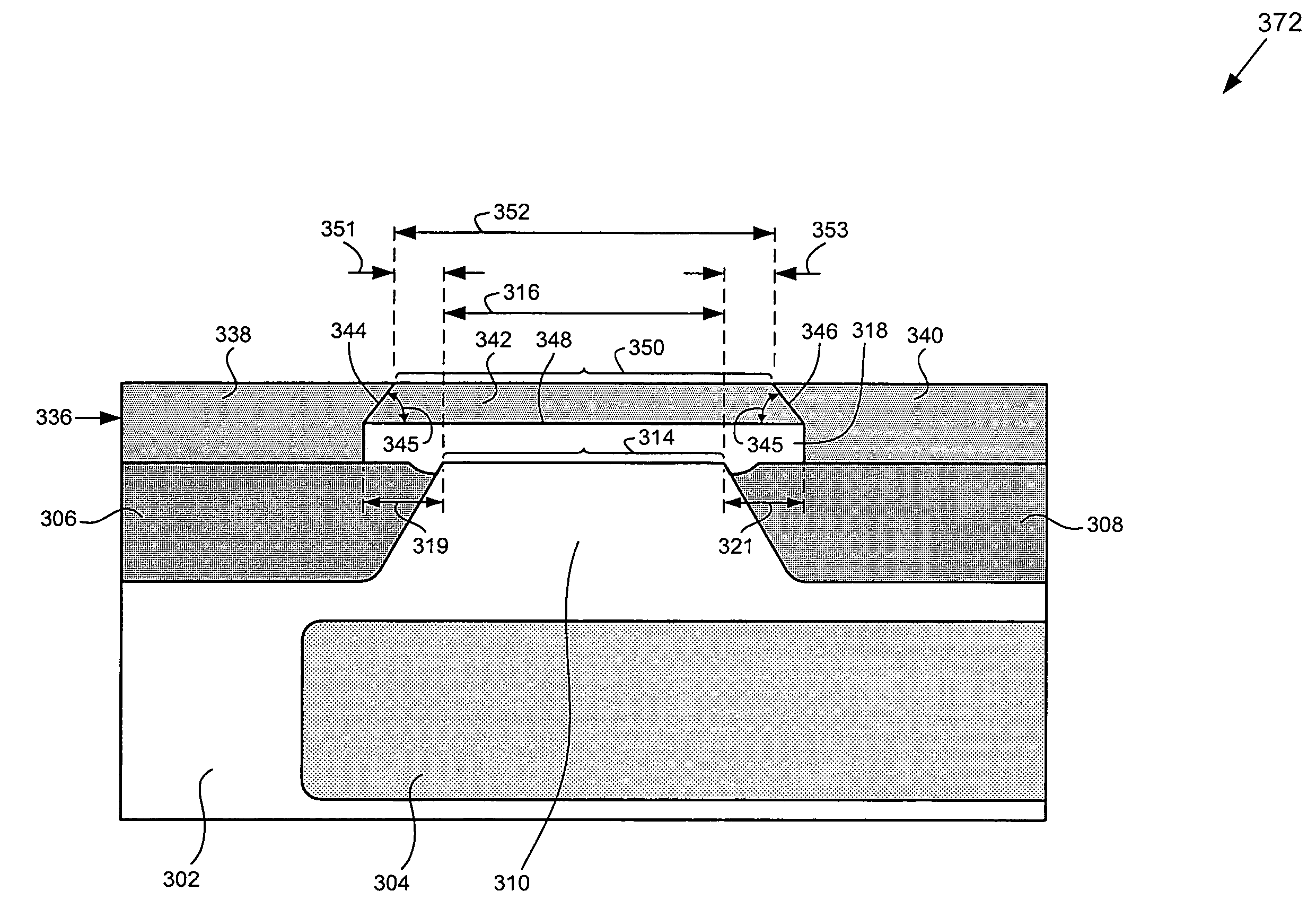
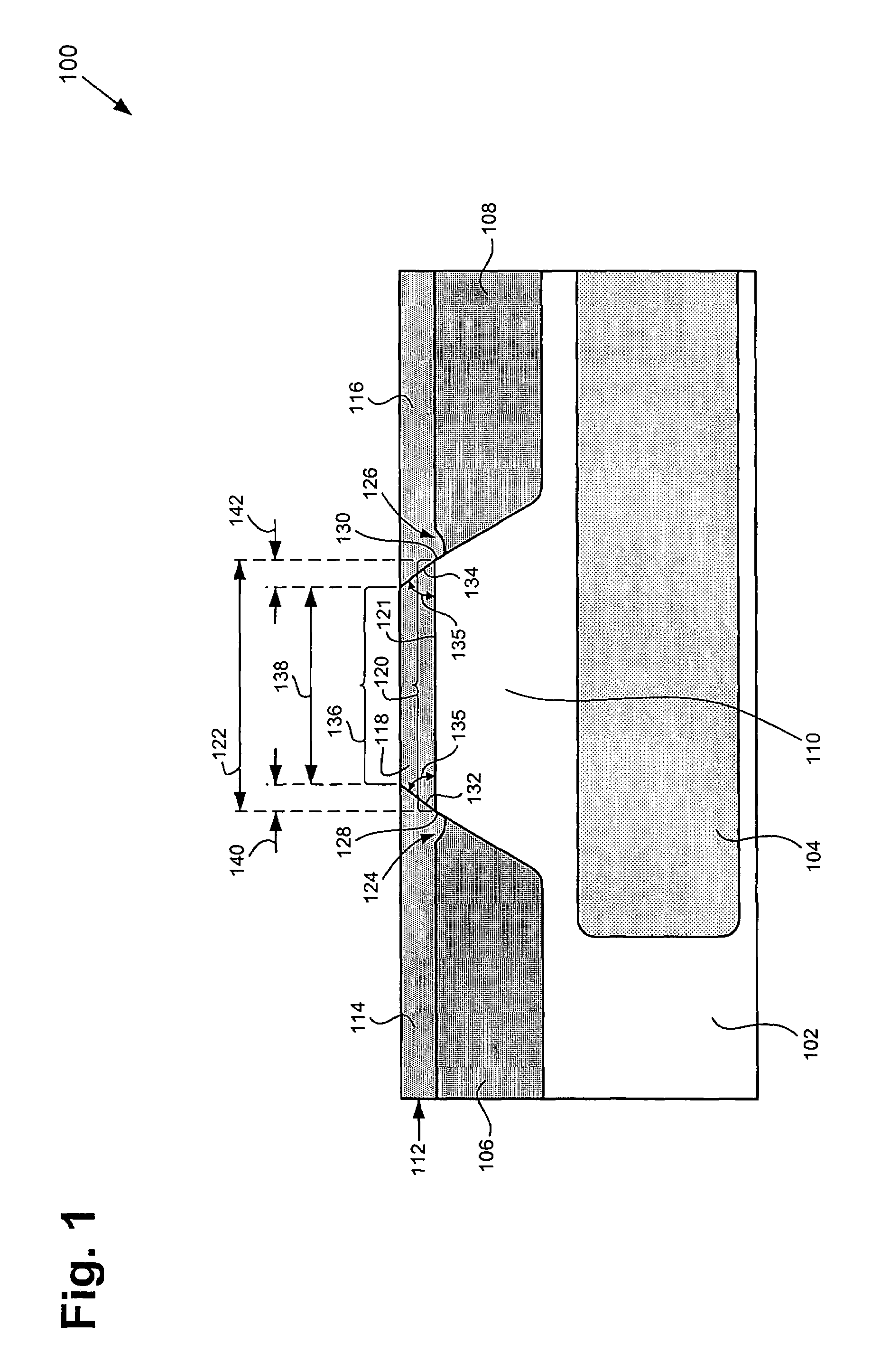
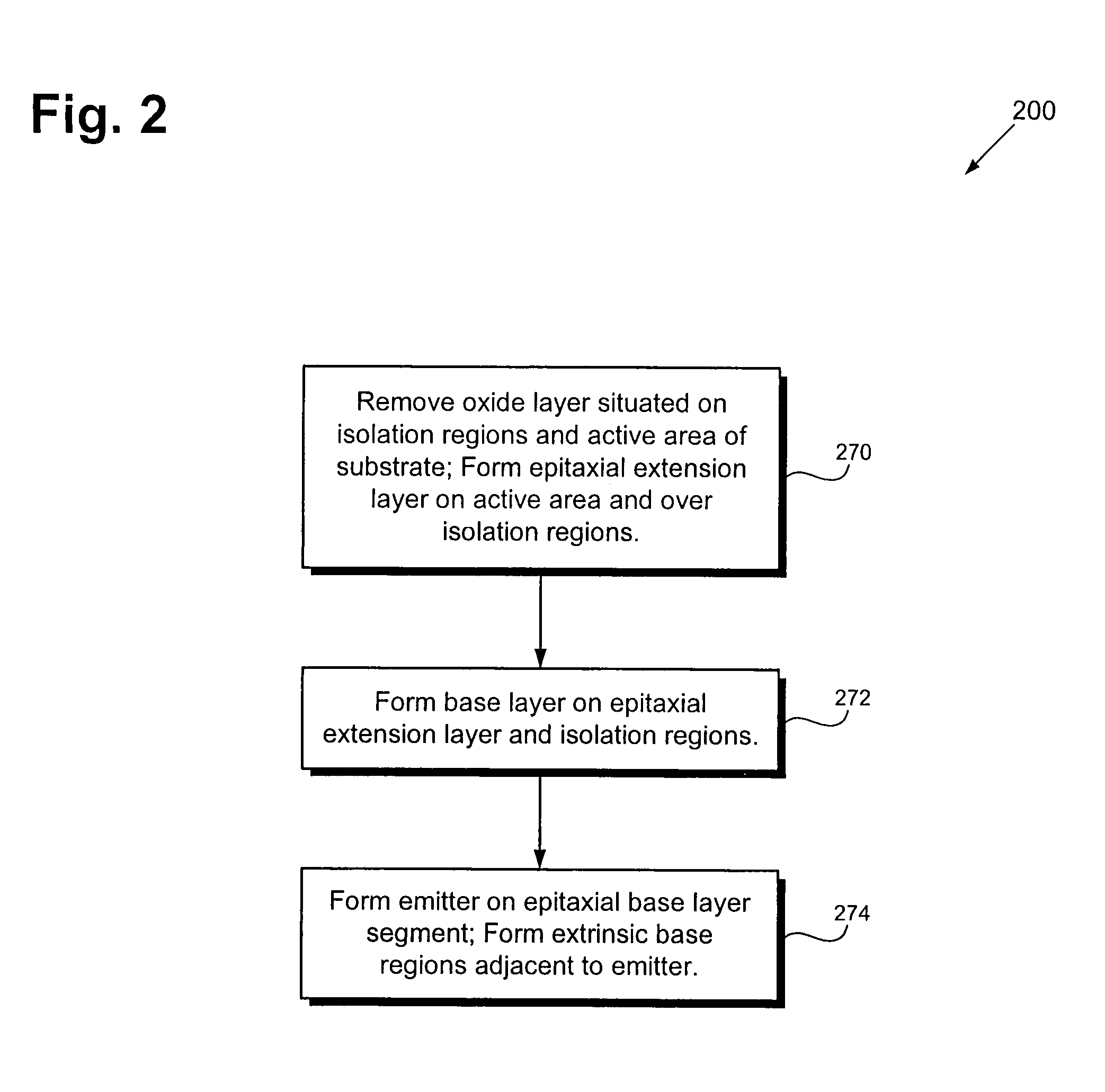
[0018]The present invention is directed to selective and non-selective epitaxy for base integration in a BiCMOS process and related structure. The following description contains specific information pertaining to the implementation of the present invention. One skilled in the art will recognize that the present invention may be implemented in a manner different from that specifically discussed in the present application. Moreover, some of the specific details of the invention are not discussed in order not to obscure the invention. The specific details not described in the present application are within the knowledge of a person of ordinary skill in the art.

[0019]The drawings in the present application and their accompanying detailed description are directed to merely exemplary embodiments of the invention. To maintain brevity, other embodiments of the invention which use the principles of the present invention are not specifically described in the present application and are not sp...


PUM


Abstract

According to one exemplary embodiment, a bipolar transistor includes an active area situated between first and second isolation regions in a substrate. The bipolar transistor further includes an epitaxial extension layer situated on the active area, where the epitaxial extension layer extends over the first and second isolation regions. The bipolar transistor further includes a base layer situated on the epitaxial extension layer, where the base layer includes an epitaxial base, and where the epitaxial base includes a usable emitter formation area. The active area has a first width and the usable emitter formation area has a second width, where the second width is at least as large as the first width.

Description

[0001]This is a continuation of application Ser. No. 11 / 146,537 filed Jun. 6, 2005 issued as U.S. Pat. No. 7,291,898.BACKGROUND OF THE INVENTION[0002]1. Field of the Invention[0003]The present invention is generally in the field of semiconductors. More specifically, the invention is in the field of bipolar and CMOS device fabrication.[0004]2. Related Art[0005]In Bipolar Complementary-Metal-Oxide-Semiconductor (“BiCMOS”) technology, active area scaling has been utilized to increase the performance of transistors, such as silicon-germanium (“SiGe”) heterojunction bipolar transistors (HBT). However, active area scaling is limited in a conventional BiCMOS integration process as a result of facet formation that occurs during a non-selective epitaxial process that is used for base layer formation. See, e.g., “Lateral Scaling Challenges for SiGe NPN BiCMOS Process Integration.” Materials Science in Semiconductor Processing, Vol. 8 (2005) pp. 313-317 by G. D. U'Ren.[0006]In a conventional B...

Claims


Application Information

Patent Timeline
Patent Type & Authority Patents(United States)
IPC IPC(8): H01L27/082
CPCH01L29/1004H01L29/66287H01L29/732H01L21/8249
Inventor U'REN, GREG D.
Owner NEWPORT FAB
Why Eureka
Try Eureka