Semiconductor memory device

a memory device and semiconductor technology, applied in the field of semiconductor memory devices, can solve the problems of data retention time suddenly degraded, reduced reliability of memory cells, and reduced product reliability

Inactive Publication Date: 2008-12-16
SOCIONEXT INC
View PDF16 Cites 38 Cited by
  • Summary
  • Abstract
  • Description
  • Claims
  • Application Information

AI Technical Summary

Benefits of technology

[0018]It is another object of the present invention to provide a semiconductor memory device capable of grasping an increase of defective bits due to deterioration with time of a memory cell.
[0019]It is yet another object of the present invention to provide a semiconductor memory device capable of correctly counting the number of error corrections.

Problems solved by technology

However, when the miniaturization technique progresses, reliability in a memory cell is reduced.
According to this technique, although the reduction in the reliability of products themselves can be prevented, the following problem occurs in recent years.
In the memory cell requiring a refresh operation, such as a DRAM cell, a data retention time is suddenly degraded, and thereby defects occur after packaging or shipping of products.
However, when the number of single-bit defects of which the repair by the redundant technique can be taken over by the ECC function is too large, a probability of repair defective bits caused by a data retention time degradation is reduced.
The conventional semiconductor memory device, however, has some problems as described hereinbelow.
Even if the number of error corrections counted during the test operation is too large or too small with respect to the set upper limit, the upper limit cannot be arbitrarily set.
Due to deterioration with time of the memory cell, the number of the defective bits after the packaging or shipping increases more than that during the test operation in some cases.

Method used


Image

  • Semiconductor memory device
  • Semiconductor memory device
  • Semiconductor memory device

Examples


first embodiment

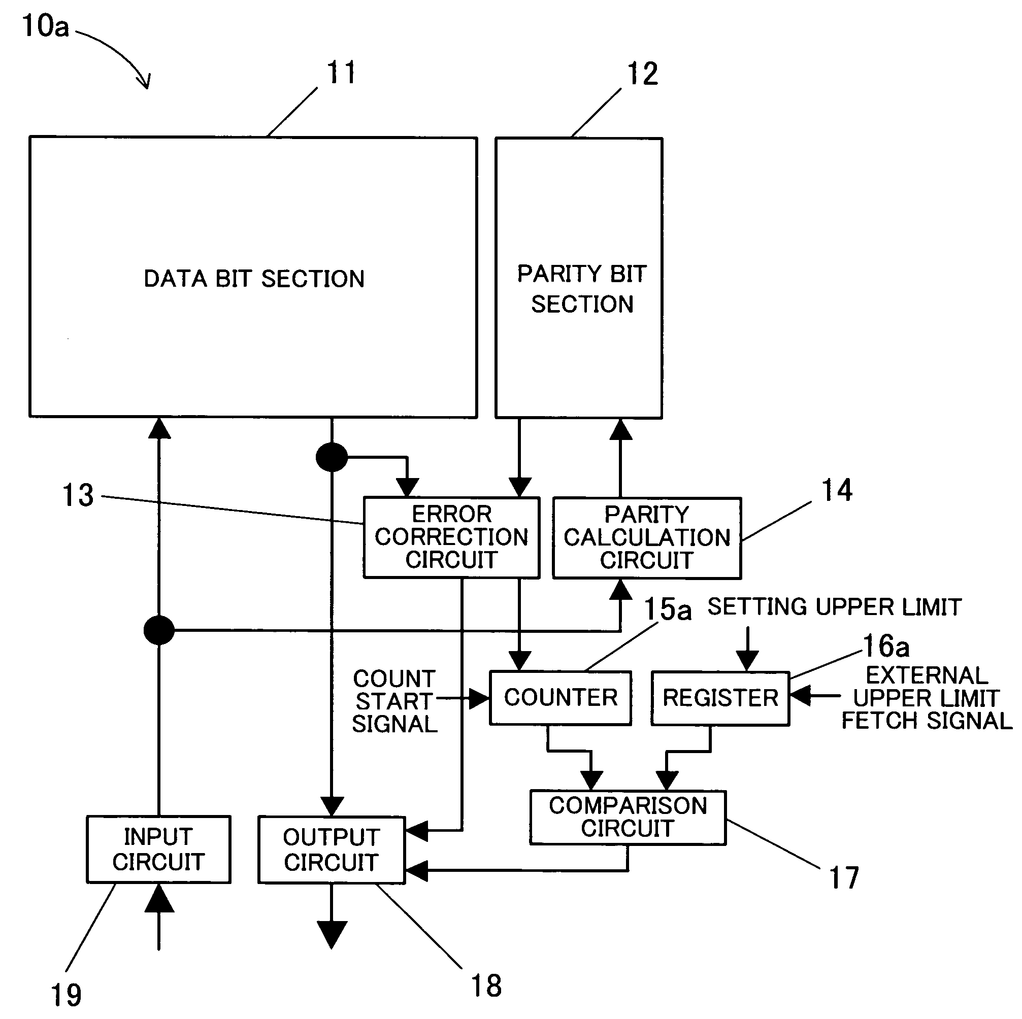
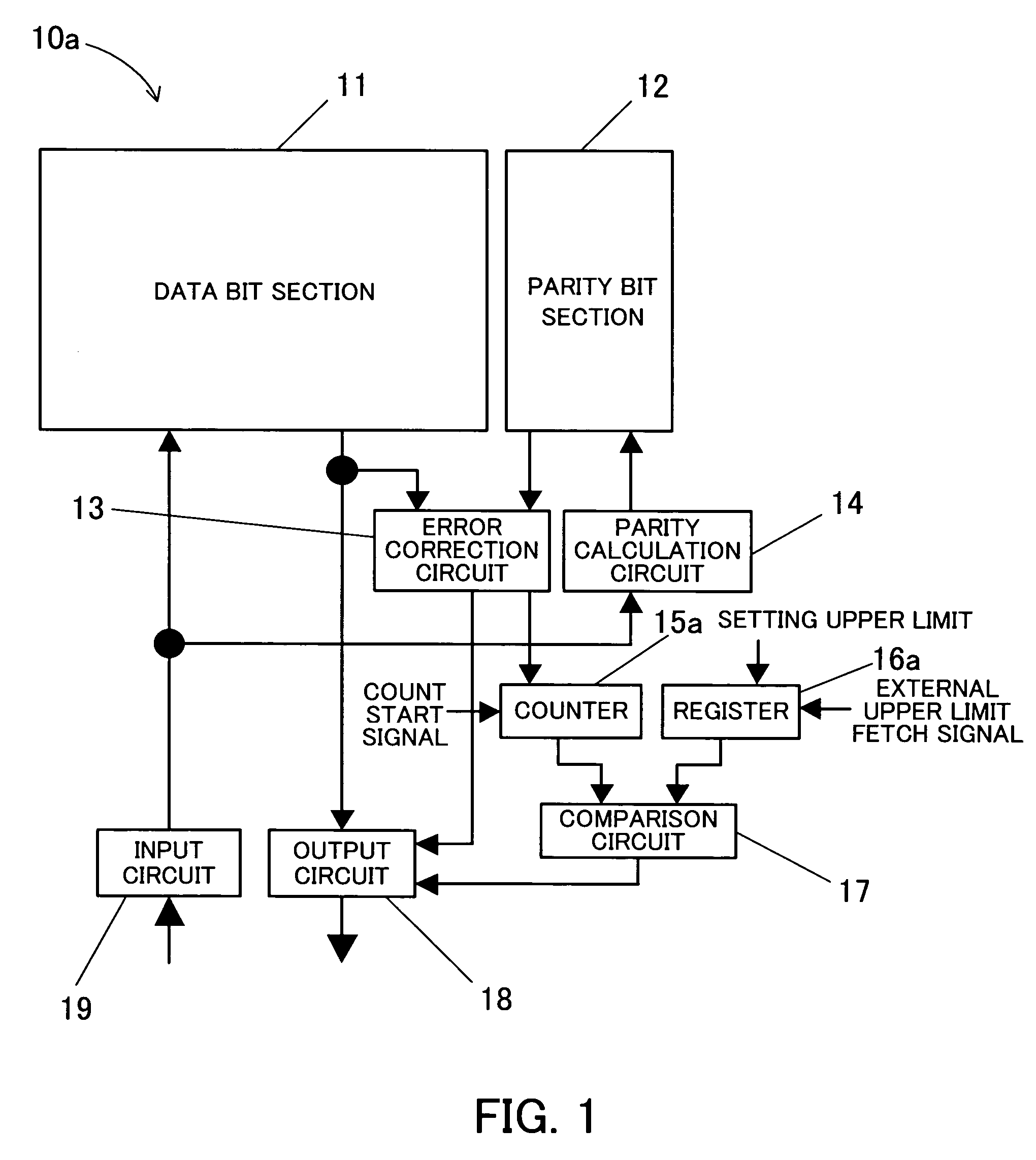
[0035]FIG. 1 shows a configuration of a semiconductor memory device according to the present invention.

[0036]The semiconductor memory device 10a of the first embodiment has the following elements: a data bit section 11 that stores a data bit; a parity bit section 12 that stores a parity bit; an error correction circuit 13 that performs an error correction with reference to the data bit and the parity bit; a parity calculation circuit 14 that generates a parity bit in response to input data by the calculation based on, for example, a hamming code; a counter 15a that counts the number of error corrections; a register 16a that sets an upper limit of the number of error corrections; a comparison circuit 17 that compares the counted number of error corrections with the upper limit of the number of error corrections stored in the register 16a; an output circuit 18; and an input circuit 19.

[0037]The data bit section 11 and the parity bit section 12 each are configured by memory cell arrays...

second embodiment

[0048]Next, the semiconductor memory device of a second embodiment is described.

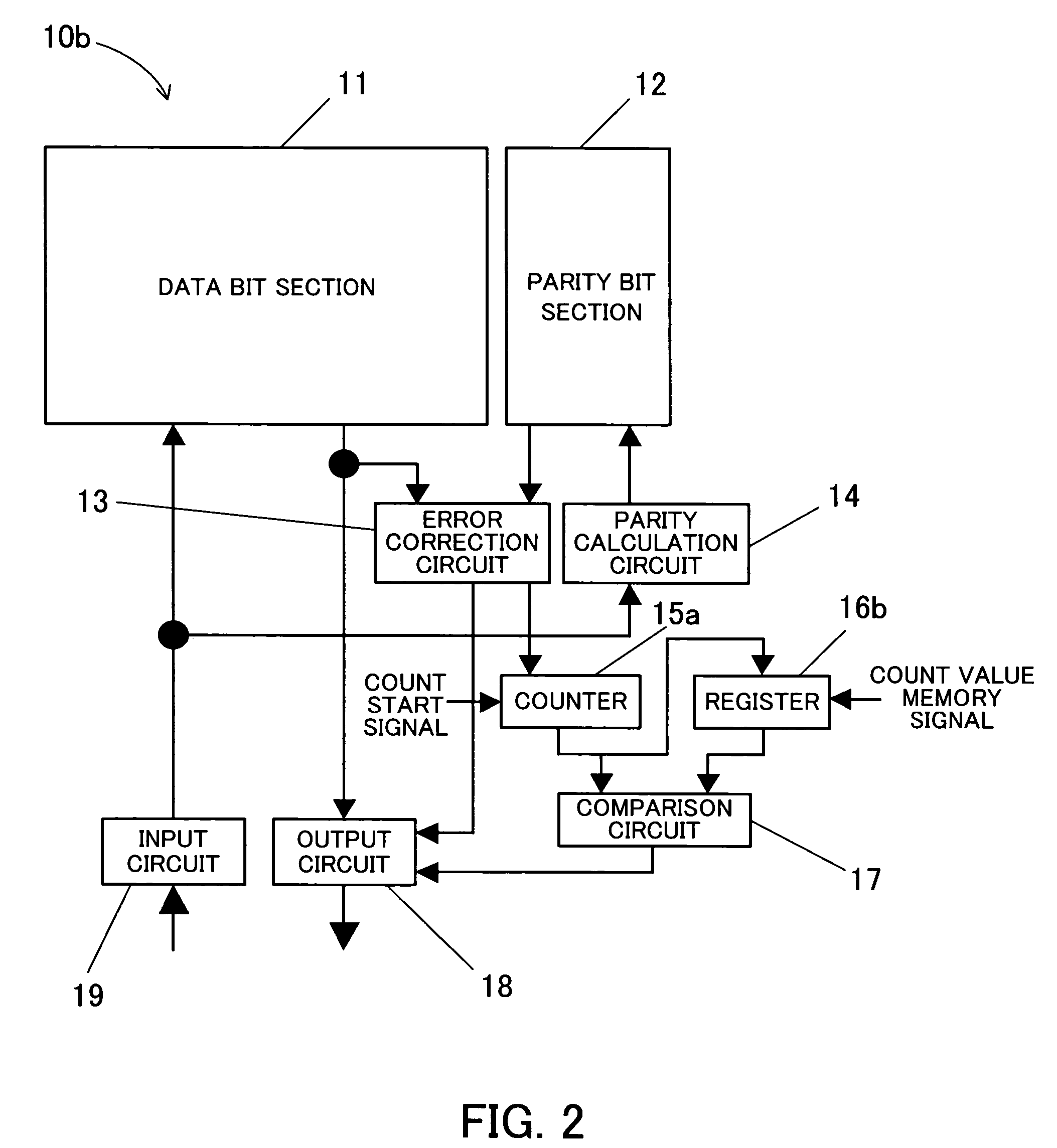
[0049]FIG. 2 shows a configuration of the semiconductor memory device according to the second embodiment of the present invention.

[0050]In the diagram, the same elements as those in the semiconductor memory device 10a of the first embodiment are indicated by the same reference numerals as in the device 10a and the description is omitted.

[0051]In the semiconductor memory device 10b of the second embodiment, a register 16b that sets an upper limit is different from the register 16a in the semiconductor memory device 10a of the first embodiment. When the upper limit setting signal (referred to as a “count value memory signal” in the second embodiment) is inputted (goes to a high level) externally, the register 16b sets a count result of the number of error corrections in the counter 15a as the upper limit of the number of error corrections.

[0052]Operations of the semiconductor memory device 10b of the secon...

third embodiment

[0055]Next, a semiconductor memory device of a third embodiment is described.

[0056]FIG. 3 shows a configuration of the semiconductor memory device according to the third embodiment of the present invention.

[0057]In the diagram, the same elements as those in the semiconductor memory devices 10a and 10b of the first and second embodiments are indicated by the same reference numerals as those in the devices 10a and 10b and the description is omitted.

[0058]In the semiconductor memory device 10c of the third embodiment, the register 16c is different from the register 16a in the semiconductor memory device 10a of the first embodiment. When the upper limit setting signal (referred to as an “upper limit increment / decrement signal” in the third embodiment) is externally inputted (goes to a high level), the register 16c increments or decrements the upper limit in synchronization with a clock signal.

[0059]Operations of the semiconductor memory device loc of the third embodiment are described b...


PUM


Abstract

Disclosed is a semiconductor memory device capable of arbitrarily setting an upper limit of the number of error corrections during a test operation. The semiconductor memory device has a counter, a register, and a comparison circuit. The counter counts the number of error corrections. The register, when an upper limit setting signal is externally inputted to change the upper limit of the number of error corrections, changes the upper limit. The comparison circuit compares the number of error corrections with the changed upper limit.

Description

CROSS-REFERENCE TO RELATED APPLICATIONS[0001]This application is based upon and claims the benefits of priority from the prior Japanese Patent Application No. 2004-370316, filed on Dec. 22, 2004, the entire contents of which are incorporated herein by reference.BACKGROUND OF THE INVENTION[0002]1. Field of the Invention[0003]The present invention relates to a semiconductor memory device, and particularly to a semiconductor memory device having an error correction function.[0004]2. Description of the Related Art[0005]In a semiconductor memory device such as a DRAM (Dynamic Random Access Memory) mounted on computer equipments, a necessary memory capacity rapidly increases in recent years. In response to the increase in memory capacity, a miniaturization technique progresses. However, when the miniaturization technique progresses, reliability in a memory cell is reduced. In order to prevent the reduction in reliability, the following redundant technique has been used. An extra memory re...

Claims


Application Information

Patent Timeline
Patent Type & Authority Patents(United States)
IPC IPC(8): G06F11/00
CPCG11C29/42G11C11/41
Inventor NAKAMURA, TOSHIKAZUKIKUTAKE, AKIRAKAWABATA, KUNINORIONISHI, YASUHIROETO, SATOSHI
Owner SOCIONEXT INC
Why Eureka
Try Eureka